


In accordance with personal data protection laws enforced by the European Union, we are committed to protecting your personal data and providing you with control over your personal data.
We have updated and will periodically update our Privacy Policy, to comply with the personal data protection. Please refer to our latest version of Privacy Policy。
This website uses cookies to provide a better browsing experience. To find out more about the cookies we use, pleas check here。
APW8869A
Active
DDR2 AND DDR3/DDR3L SYNCHRONOUS BUCK CONTROLLER WITH 1.5A LDO SUPPORT LOW IQ
Features
Buck Controller (VDDQ)
- Adjustable Switching Frequency from 400kHz to 550kHz in PWM Mode with DC Output Current
General Description
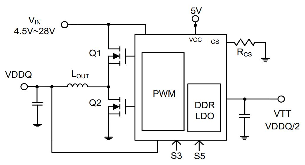
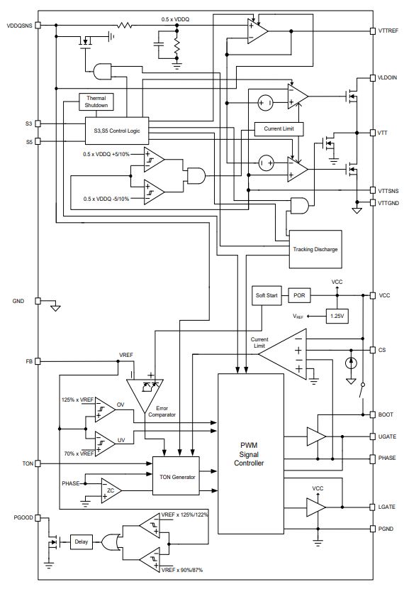
The APW8869A integrates a synchronous buck PWM controller to generate VDDQ, a sourcing and sinking LDO linear regulator to generate VTT. It offers the lowest total solution cost in system where space is at a premium. The APW8869A provides excellent transient response and accurate DC voltage output in either PFM or PWM Mode. In Pulse Frequency Mode (PFM), the APW8869A provides very high efficiency over light to heavy loads with loadingmodulated switching frequencies. On TQFN-20 Package, the Forced PWM Mode works nearly at constant frequency for low-noise requirements. The APW8869A is equipped with accurate current-limit, output under-voltage, and output over-voltage protections. A Power-On- Reset function monitors the voltage on VCC prevents wrong operation during power on. The LDO is designed to provide a regulated voltage with bi-directional output current for DDR-SDRAM termination. The device integrates two power transistors to source or sink current up to 1.5A. It also incorporates current-limit and thermal shutdown protection. The output voltage of LDO tracks the voltage at VREF pin. An internal resistor divider is used to provide a half voltage of VREF for VTTREF and VTT Voltage. The VTT output voltage is only requiring 20µF of ceramic output capacitance for stability and fast transient response. The S3 and S5 pins provide the sleep state for VTT (S3 state) and suspend state (S4/S5 state) for device, when S5 and S3 are both pulled low the device provides the soft-off for VTT and VTTREF.
Features
Buck Controller (VDDQ)
- High Input Voltages Range from 4.5V to 28V Input Power
- Provide Adjustable Output Voltage from 0.9V to 2V +1% Accuracy over Temperature
- Integrated MOSFET Drivers and Bootstrap Forward P-CH MOSFET
- Low Quiescent Current (200µA)
- Excellent Line and Load Transient Responses
- PFM Mode for Increased Light Load Efficiency
- Constant On-Time Controller Scheme
- Adjustable Switching Frequency from 400kHz to 550kHz in PWM Mode with DC Output Current
- S3 and S5 Pins Control The Device in S0, S3 or S4/S5 State
- Power Good Monitoring
- 70% Under-Voltage Protection (UVP)
- 125% Over-Voltage Protection (OVP)
- Adjustable Current-Limit Protection
- TQFN-20 3mmx3mm Thin package
- Lead Free Available (RoHS Compliant) ±1.5A LDO Section (VTT)
- Sourcing or Sinking Current up to 1.5A
- Fast Transient Response for Output Voltage
- Output Ceramic Capacitors Support at least 10µF MLCC
- VTT and VTTREF Track at Half the VDDQSNS by internal divider
- ±20mV Accuracy for VTT and VTTREF
- Independent Over-Current Limit (OCL)
- Thermal Shutdown Protection
General Description
The APW8869A integrates a synchronous buck PWM controller to generate VDDQ, a sourcing and sinking LDO linear regulator to generate VTT. It offers the lowest total solution cost in system where space is at a premium. The APW8869A provides excellent transient response and accurate DC voltage output in either PFM or PWM Mode. In Pulse Frequency Mode (PFM), the APW8869A provides very high efficiency over light to heavy loads with loadingmodulated switching frequencies. On TQFN-20 Package, the Forced PWM Mode works nearly at constant frequency for low-noise requirements. The APW8869A is equipped with accurate current-limit, output under-voltage, and output over-voltage protections. A Power-On- Reset function monitors the voltage on VCC prevents wrong operation during power on. The LDO is designed to provide a regulated voltage with bi-directional output current for DDR-SDRAM termination. The device integrates two power transistors to source or sink current up to 1.5A. It also incorporates current-limit and thermal shutdown protection. The output voltage of LDO tracks the voltage at VREF pin. An internal resistor divider is used to provide a half voltage of VREF for VTTREF and VTT Voltage. The VTT output voltage is only requiring 20µF of ceramic output capacitance for stability and fast transient response. The S3 and S5 pins provide the sleep state for VTT (S3 state) and suspend state (S4/S5 state) for device, when S5 and S3 are both pulled low the device provides the soft-off for VTT and VTTREF.