


依據歐盟施行的個人資料保護法,我們致力於保護您的個人資料並提供您對個人資料的掌握。 我們已更新並將定期更新我們的隱私權政策,以遵循該個人資料保護法。請您參照我們最新版的 隱私權聲明。
本網站使用cookies以提供更好的瀏覽體驗。如需了解更多關於本網站如何使用cookies 請按 這裏。
APW8863
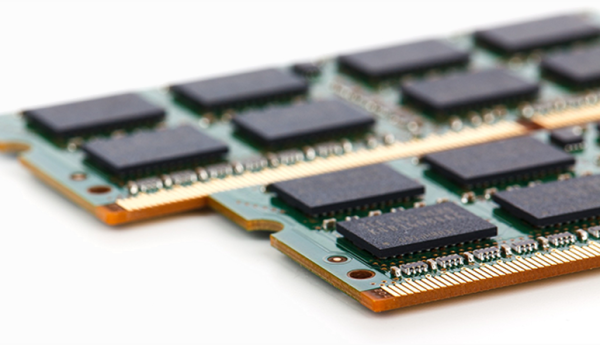
DDR3 AND DDR4 SYNCHRONOUS BUCK CONTVERTER WITH 1.5A LDO
Features
Buck Controller (VDDQ)
- Adjustable Switching Frequency from 400kHz to 550kHz in PWM Mode with DC Output Current
General Description
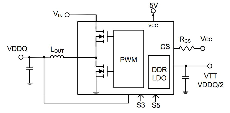
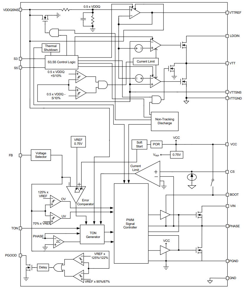
The APW8863 integrates a synchronous buck PWM converter to generate VDDQ, a sourcing and sinking LDO linear regulator to generate VTT. It offers the lowest total solution cost in system where space is at a premium. The APW8863 provides excellent transient response and accurate DC voltage output in either PFM or PWM Mode. In Pulse Frequency Mode (PFM), the APW8863 provides very high efficiency over light to heavy loads with loading-modulated switching frequencies. On TQFN-32 Package, the Forced PWM Mode works nearly at constant frequency for low-noise requirements. The APW8863 is equipped with accurate current-limit, output under-voltage, and output over-voltage protections. A Power-On-Reset function monitors the voltage on VCC prevents wrong operation during power on. The LDO is designed to provide a regulated voltage with bi-directional output current for DDR-SDRAM termination. The device integrates two power transistors to source or sink current up to 1.5A. It also incorporates current-limit and thermal shutdown protection. The output voltage of LDO tracks the voltage at VREF pin. An internal resistor divider is used to provide a half voltage of VREF for VTTREF and VTT Voltage. The VTT output voltage is only requiring 20µF of ceramic output capacitance for stability and fast transient response. The S3 and S5 pins provide the sleep state for VTT (S3 state) and suspend state (S4/S5 state) for device, when S5 and S3 are both pulled low the device provides the soft-off for VTT and VTTREF.
Features
Buck Controller (VDDQ)
- High Input Voltages Range from 4.5V to 21V Input Power
- Provide Adjustable Output Voltage from 0.9V to 2V
- Integrated MOSFET Drivers and Bootstrap Forward P-CH MOSFET
- Low Quiescent Current (200uA)
- Excellent Load Transient Responses
- PFM Mode for Increased Light Load Efficiency
- Constant On-Time Controller Scheme
- Adjustable Switching Frequency from 400kHz to 550kHz in PWM Mode with DC Output Current
- S3 and S5 Pins Control The Device in S0, S3 or S4/ S5 State
- Power Good Monitoring
- 70% Under-Voltage Protection (UVP)
- 125% Over-Voltage Protection (OVP)
- Adjustable Current-Limit Protection
- TQFN-32 4mmx4mm Thin package
- Lead Free Available (RoHS Compliant)
- ±1.5A LDO Section (VTT)
- Souring or Sinking Current up to 1.5A
- Fast Transient Response for Output Voltage
- Output Ceramic Capacitors Support at least 10µF MLCC
- VTT and VTTREF Track at Half the VDDQSNS by internal divider
- ±20mV Accuracy for VTT and VTTREF
- Independent Over-Current Limit (OCL)
- Thermal Shutdown Protection
General Description
The APW8863 integrates a synchronous buck PWM converter to generate VDDQ, a sourcing and sinking LDO linear regulator to generate VTT. It offers the lowest total solution cost in system where space is at a premium. The APW8863 provides excellent transient response and accurate DC voltage output in either PFM or PWM Mode. In Pulse Frequency Mode (PFM), the APW8863 provides very high efficiency over light to heavy loads with loading-modulated switching frequencies. On TQFN-32 Package, the Forced PWM Mode works nearly at constant frequency for low-noise requirements. The APW8863 is equipped with accurate current-limit, output under-voltage, and output over-voltage protections. A Power-On-Reset function monitors the voltage on VCC prevents wrong operation during power on. The LDO is designed to provide a regulated voltage with bi-directional output current for DDR-SDRAM termination. The device integrates two power transistors to source or sink current up to 1.5A. It also incorporates current-limit and thermal shutdown protection. The output voltage of LDO tracks the voltage at VREF pin. An internal resistor divider is used to provide a half voltage of VREF for VTTREF and VTT Voltage. The VTT output voltage is only requiring 20µF of ceramic output capacitance for stability and fast transient response. The S3 and S5 pins provide the sleep state for VTT (S3 state) and suspend state (S4/S5 state) for device, when S5 and S3 are both pulled low the device provides the soft-off for VTT and VTTREF.