


依據歐盟施行的個人資料保護法,我們致力於保護您的個人資料並提供您對個人資料的掌握。 我們已更新並將定期更新我們的隱私權政策,以遵循該個人資料保護法。請您參照我們最新版的 隱私權聲明。
本網站使用cookies以提供更好的瀏覽體驗。如需了解更多關於本網站如何使用cookies 請按 這裏。
首頁
產品資訊
產品搜尋
SEARCH
產品類別
APW7715
Active
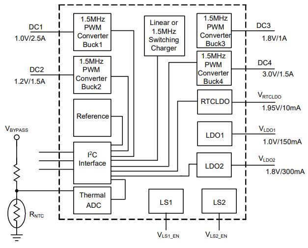
2 Buck Converter+ 1 LDO PMIC for SD Express
Features
General Description
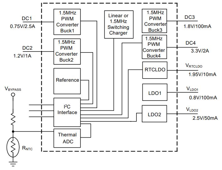
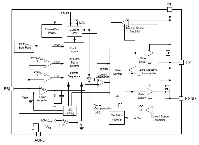
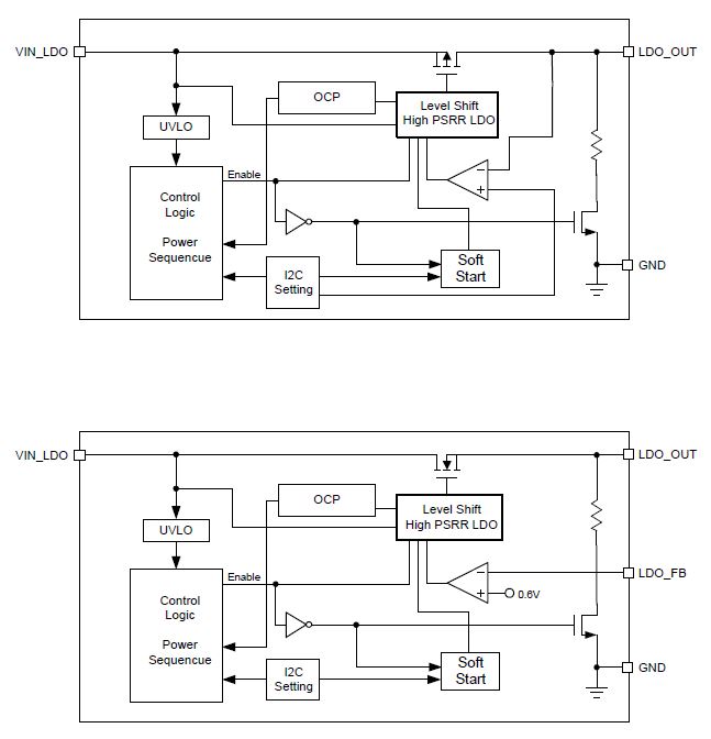
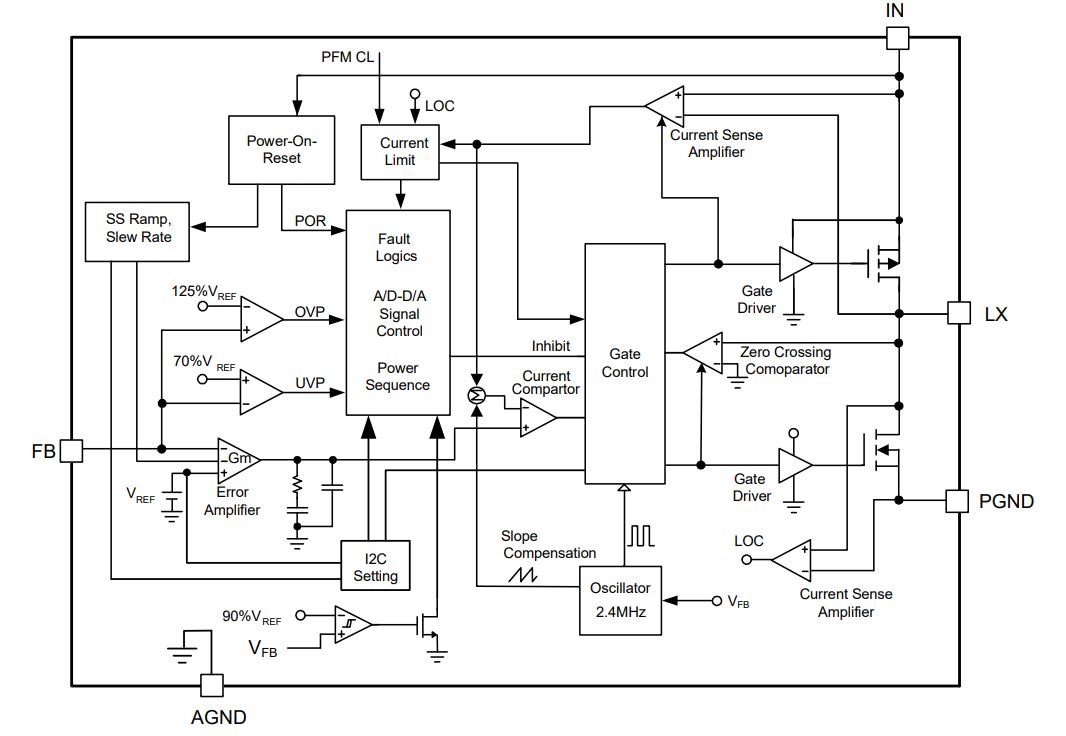
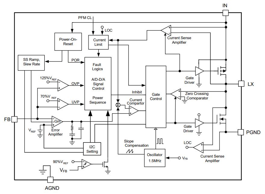
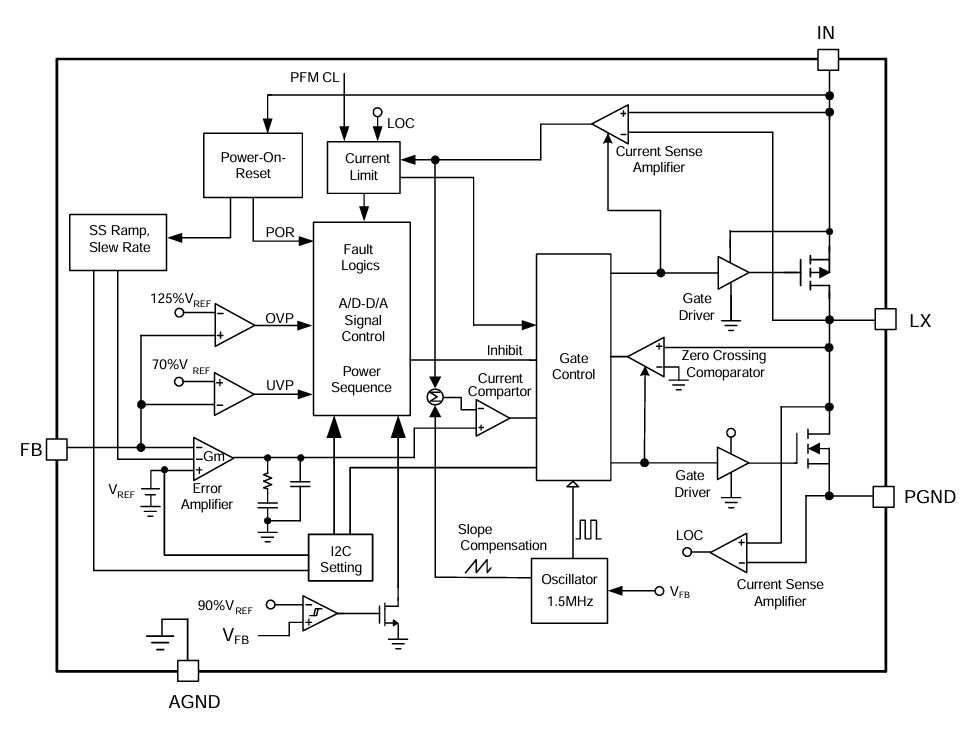
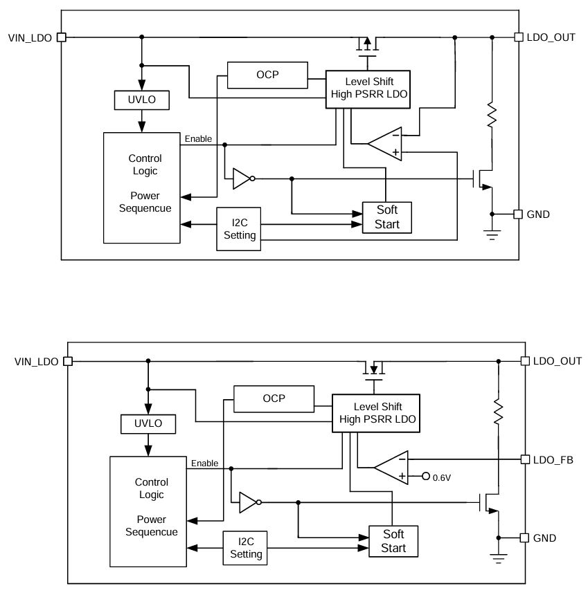
The APW7715 device is a power management solution for SD Express that integrates two high-efficiency, stepdown, DC/DC converters, one low-dropout regulator, and a flexible logic interface optimized for small solution size and high efficiency. Each DC/DC regulator switches at 2.2MHz, requiring only three small components for operation. The LDO only require small ceramic capacitors. It is highly flexible and can be reconfigured via I2C for multiple applications without the need for PCB changes. The low external component count and high configurability significantly speed time to market. Examples of configurable options include output voltage, sleep modes, input power selection for Buck2 etc.
Features
- Input Operating Range: 2.5V ~ 3.63V
- Provide Input Voltage Source Seamlessly Switched
- Built-In 2-ch Synchronous Buck Converters, 1-ch LDO
- Customized Power-On Sequence for PS5017 Controller
- Device Sleep Mode Control Pin
- Built-In Discharge Behavior
- Over-Temperature Protection
- 2.2MHz Switching Frequency for Smaller Inductor Size and Output Capacitor Size
- I2C Interface
General Description
The APW7715 device is a power management solution for SD Express that integrates two high-efficiency, stepdown, DC/DC converters, one low-dropout regulator, and a flexible logic interface optimized for small solution size and high efficiency. Each DC/DC regulator switches at 2.2MHz, requiring only three small components for operation. The LDO only require small ceramic capacitors. It is highly flexible and can be reconfigured via I2C for multiple applications without the need for PCB changes. The low external component count and high configurability significantly speed time to market. Examples of configurable options include output voltage, sleep modes, input power selection for Buck2 etc.
APW7720
Active
The PMIC Features 7 Buck Converters, 6 LDOs, 2 LSs, and Flexible System Settings Via I2C and MTP
Features
Charger
- BUCK2: 1V ~ 3.4V, 10mV Step, 2A
- BUCK3: 0.45V ~ 1.275V, 3.75mV Step, 6A
- BUCK4: 0.6V ~ 1.54V, 5mV Step, 3A
- BUCK5: 0.45V ~ 1.275V, 3.75mV Step, 3A
- BUCK6: 1V ~ 3.4V, 10mV Step, 2A
- BUCK7: 1V ~ 3.4V, 10mV Step, 2A
- LDO2: 1V ~ 3.4V, 50mV Step, 300mA
- LDO3: 1V ~ 3.4V, 50mV Step, 300mA
- LDO4: 0.6V ~ 1.23V, 10mV Step, 200mA
- LDO5: 1V ~ 3.4V, 50mV Step, 150mA
- LDO6: 0.6V ~ 1.23V, 10mV Step, 300mA
General Description
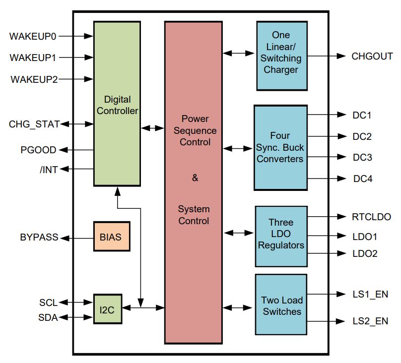
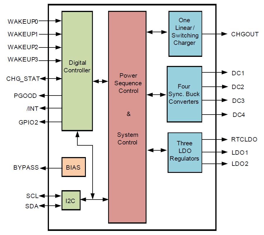
The APW7720 is a Power Management IC (PMIC) designed to provide complete power management solution for Surveillance Cam, IP Cam and Video Conference-Call applications. It integrates a PWM power stage and well-designed control circuitry to minimize the need for external components, thereby simplifying layout in constrained PCB areas. This device features 7 adjustable output voltage buck converters, 6 adjustable output voltage low-noise LDOs, and 2 sets of built-in logic control signal outputs selectable at 1.8V or 3.3V, all of which can be configured via I2C. The APW7720 features protection functions against over current, output over/under voltage, VSYS over voltage and over temperature to prevent catastrophic failure. Fault events also cause a state change on the PGOOD and /INT output pins, which is helpful for interrupt control or debugging. Additionally, it integrates two Under-Voltage Lockout (UVLO) features to monitor the voltages of VSYS and VINLDO1, thereby preventing improper operation during power-up and power-down. An I2C interface is provided in this device for the system designer to customize settings or presets using Multi-Time Programmable (MTP) features, including power-up/down sequence, output voltage, ramp-up/down time, power-good delay time, watchdog timer, PWM switching frequency, forced PWM mode or automatic PFM/PWM mode, output discharge mode or ramp-down mode, and latch off mode or auto-reboot mode. These customizable MTP settings give system designers the flexibility to optimize performance for various use cases, ensuring efficient and reliable operation. The APW7720 is halogen and lead free device, compliant with RoHS, available in TQFN6x6-52B package.
Features
Charger
- 3.5V to 5.5V Operating Input Range
- Built-in UVLO, OVP for Main Input Voltage
- Built-in 7 High-Efficiency Step-Down Converters
- BUCK2: 1V ~ 3.4V, 10mV Step, 2A
- BUCK3: 0.45V ~ 1.275V, 3.75mV Step, 6A
- BUCK4: 0.6V ~ 1.54V, 5mV Step, 3A
- BUCK5: 0.45V ~ 1.275V, 3.75mV Step, 3A
- BUCK6: 1V ~ 3.4V, 10mV Step, 2A
- BUCK7: 1V ~ 3.4V, 10mV Step, 2A
- Configurable Dual Phase or Single Phase Regulator for BUCK1/BUCK3
- Configurable PWM Switching Frequency from 400kHz to 2.5MHz
- Programmable Automatic PFM/PWM Mode, Forced PWM Mode
- Adjustable Ramp-Up Time and Ramp-Down Time for BUCK1 ~ BUCK7
- Built-in RTC Dedicated LDO and 5 Low-Noise LDOs
- LDO2: 1V ~ 3.4V, 50mV Step, 300mA
- LDO3: 1V ~ 3.4V, 50mV Step, 300mA
- LDO4: 0.6V ~ 1.23V, 10mV Step, 200mA
- LDO5: 1V ~ 3.4V, 50mV Step, 150mA
- LDO6: 0.6V ~ 1.23V, 10mV Step, 300mA
- Configurable LDO2/3 Output 1.8V/3.3V by LDO2/3_SEL Pin
- Built-in Dual Sets of Logic Control Signal Outputs, Selectable at 1.8V or 3.3V
- Built-in Double Thermal Protection with Temperature Alarm and Thermal Shutdown
- Built-in Output Over Voltage Protection (OVP), Output Under Voltage Protection (UVP), Current Limit
- Built-in Interrupt Control and Reporting by /INT Pin
- Built-in PGOOD to Indicate the Power Status of All VRs
- I2C Bus and User Programmable MTP
- Programmable Power Sequence Control for All Channels Via I2C
- Built-in Watchdog Timer, Programmable Via I2C
- Supports Self-Refresh Mode Via Off Mode Function
- Available in TQFN6x6-52B Package
General Description
The APW7720 is a Power Management IC (PMIC) designed to provide complete power management solution for Surveillance Cam, IP Cam and Video Conference-Call applications. It integrates a PWM power stage and well-designed control circuitry to minimize the need for external components, thereby simplifying layout in constrained PCB areas. This device features 7 adjustable output voltage buck converters, 6 adjustable output voltage low-noise LDOs, and 2 sets of built-in logic control signal outputs selectable at 1.8V or 3.3V, all of which can be configured via I2C. The APW7720 features protection functions against over current, output over/under voltage, VSYS over voltage and over temperature to prevent catastrophic failure. Fault events also cause a state change on the PGOOD and /INT output pins, which is helpful for interrupt control or debugging. Additionally, it integrates two Under-Voltage Lockout (UVLO) features to monitor the voltages of VSYS and VINLDO1, thereby preventing improper operation during power-up and power-down. An I2C interface is provided in this device for the system designer to customize settings or presets using Multi-Time Programmable (MTP) features, including power-up/down sequence, output voltage, ramp-up/down time, power-good delay time, watchdog timer, PWM switching frequency, forced PWM mode or automatic PFM/PWM mode, output discharge mode or ramp-down mode, and latch off mode or auto-reboot mode. These customizable MTP settings give system designers the flexibility to optimize performance for various use cases, ensuring efficient and reliable operation. The APW7720 is halogen and lead free device, compliant with RoHS, available in TQFN6x6-52B package.
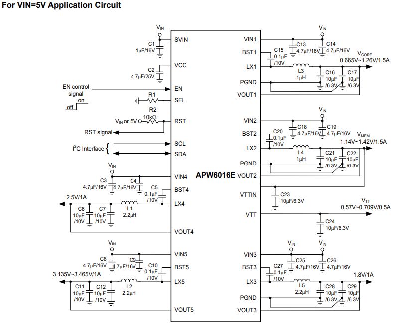
APW6016
Active
5 Buck Converters and 1 Termination LDO PMIC with I2C Interface
Features
- 1.5A output current capability
- 750KHz / 1.5MHz switching frequency
- 1.5A output current capability
- 750KHz / 1.5MHz switching frequency
- 1.0A output current capability
- 750KHz / 1.5MHz switching frequency
- 1.0A output current capability
- 750KHz / 1.5MHz switching frequency
- 1.0A output current capability
- 750KHz / 1.5MHz switching frequency
General Description
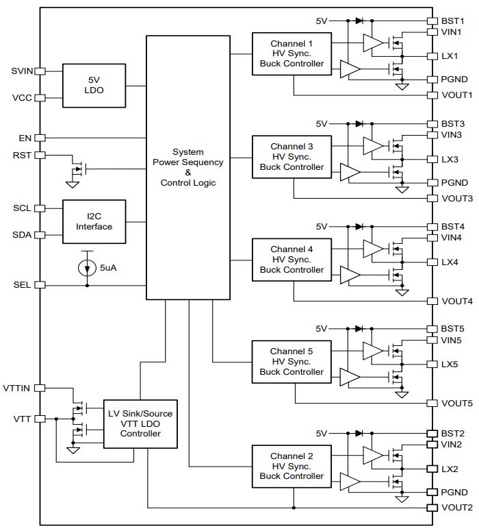
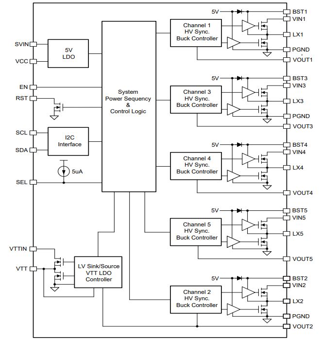
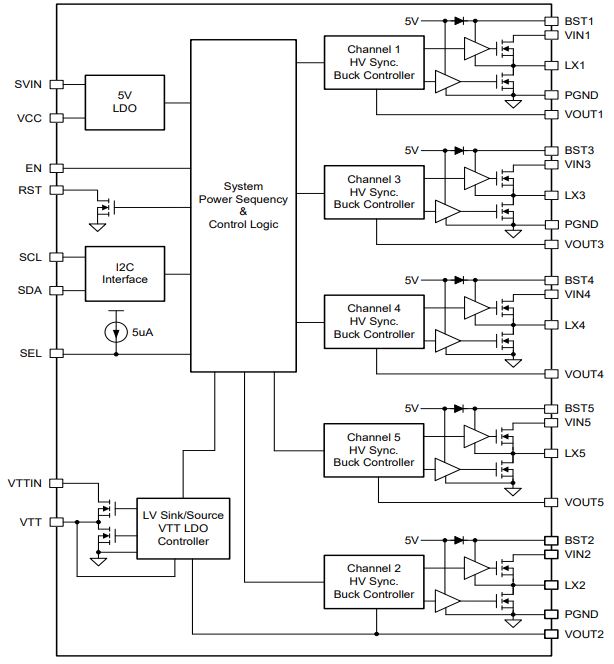
The APW6016 is designed for server management processor power system, which integrates 5 buck converters and one 0.5A sink/source VTT LDO into one single package. The PWM converters and VTT LDO output voltage can support VCORE, memory, memory bus termination and 1.8V/2.5V/3.3V I/O. Each VR voltage are programmable with high resolution via I2C interface. Moreover, the power-on and power-off sequences as well as soft-start time of these VR are controlled and programmable via I2C interface, providing versatility for system designers. The APW6016 provides excellent transient response and accurate DC voltage output in either PFM or PWM Mode. In Pulse Frequency Modulation mode (PFM), the APW6016 provides very high efficiency over light to heavy loads with loading-modulated switching frequencies. On VTQFN-32 Package, the Forced PWM Mode works nearly at constant frequency for low-noise requirements. The APW6016 features sufficient protections against over-current, over-voltage, short circuit and over-temperature to prevent catastrophic failure. A Power-On-Reset function monitors the voltage on SVIN prevents wrong operation during power on. The output voltage of VTT automatically tracks the voltage of half VOUT2. The VTT output voltage is only requiring 10µF of ceramic output capacitance for stability and fast transient response.
Features
- High Input Voltages Range from 4.5V to 16V
- Built in Input Voltage UVLO threshold
- Built in VIN OVP
- Programmable power sequence control by I2C for all channel
- Provide 5 Single-Buck PWM Converter and 1 Termination LDO Regulator
- Channel 1 Synchronous Buck for VCORE (Default 1V)
- 1.5A output current capability
- 750KHz / 1.5MHz switching frequency
- Channel 2 Synchronous Buck for Memory (Default 1.2V)
- 1.5A output current capability
- 750KHz / 1.5MHz switching frequency
- Channel 3 Synchronous Buck for I/O (Default 1.8V)
- 1.0A output current capability
- 750KHz / 1.5MHz switching frequency
- Channel 4 Synchronous Buck for I/O (Default 2.5V)
- 1.0A output current capability
- 750KHz / 1.5MHz switching frequency
- Channel 5 Synchronous Buck for I/O (Default 3.3V)
- 1.0A output current capability
- 750KHz / 1.5MHz switching frequency
- Channel 6 VTT Termination LDO Regulator
- Built-in EN function
- Built-in RST to monitor output voltage status
- Built-in Current Limit/SCP/OVP/OTP
- VTQFN-32 4mmx4mm Thin package
- Lead Free Available (RoHS Compliant)
General Description
The APW6016 is designed for server management processor power system, which integrates 5 buck converters and one 0.5A sink/source VTT LDO into one single package. The PWM converters and VTT LDO output voltage can support VCORE, memory, memory bus termination and 1.8V/2.5V/3.3V I/O. Each VR voltage are programmable with high resolution via I2C interface. Moreover, the power-on and power-off sequences as well as soft-start time of these VR are controlled and programmable via I2C interface, providing versatility for system designers. The APW6016 provides excellent transient response and accurate DC voltage output in either PFM or PWM Mode. In Pulse Frequency Modulation mode (PFM), the APW6016 provides very high efficiency over light to heavy loads with loading-modulated switching frequencies. On VTQFN-32 Package, the Forced PWM Mode works nearly at constant frequency for low-noise requirements. The APW6016 features sufficient protections against over-current, over-voltage, short circuit and over-temperature to prevent catastrophic failure. A Power-On-Reset function monitors the voltage on SVIN prevents wrong operation during power on. The output voltage of VTT automatically tracks the voltage of half VOUT2. The VTT output voltage is only requiring 10µF of ceramic output capacitance for stability and fast transient response.
APW6016B
Active
5 Buck Converters and 1 Termination LDO PMIC with I2C Interface
Features
- 1.5A output current capability
- 750KHz / 1.5MHz switching frequency
- 1.5A output current capability
- 750KHz / 1.5MHz switching frequency
- 1.0A output current capability
- 750KHz / 1.5MHz switching frequency
- 1.0A output current capability
- 750KHz / 1.5MHz switching frequency
- 1.0A output current capability
- 750KHz / 1.5MHz switching frequency
General Description
The APW6016B is designed for server management processor power system, which integrates 5 buck converters and one 0.5A sink/source VTT LDO into one single package. The PWM converters and VTT LDO output voltage can support VCORE, memory, memory bus termination and 1.2V/1.85V/3.3V I/O. Each VR voltage are programmable with high resolution via I2C interface. Moreover, the power-on and power-off sequences as well as soft-start time of these VR are controlled and programmable via I2C interface, providing versatility for system designers. The APW6016B provides excellent transient response and accurate DC voltage output in either PFM or PWM Mode. In Pulse Frequency Modulation mode (PFM), the APW6016B provides very high efficiency over light to heavy loads with loading-modulated switching frequencies. On VTQFN-32 Package, the Forced PWM Mode works nearly at constant frequency for low-noise requirements. The APW6016B features sufficient protections against over-current, over-voltage, short circuit and over-temperature to prevent catastrophic failure. A Power-On-Reset function monitors the voltage on SVIN prevents wrong operation during power on. The output voltage of VTT automatically tracks the voltage of half VOUT2. The VTT output voltage is only requiring 10µF of ceramic output capacitance for stability and fast transient response.
Features
- High Input Voltages Range from 4.5V to 16V
- Built in Input Voltage UVLO threshold
- Built in VIN OVP
- Programmable power sequence control by I2C for all channel
- Provide 5 Single-Buck PWM Converter and 1 Termination LDO Regulator
- Channel 1 Synchronous Buck for VCORE (Default 1.275V)
- 1.5A output current capability
- 750KHz / 1.5MHz switching frequency
- Channel 2 Synchronous Buck for Memory (Default 1.3V)
- 1.5A output current capability
- 750KHz / 1.5MHz switching frequency
- Channel 3 Synchronous Buck for I/O (Default 1.85V)
- 1.0A output current capability
- 750KHz / 1.5MHz switching frequency
- Channel 4 Synchronous Buck for I/O (Default 3.3V)
- 1.0A output current capability
- 750KHz / 1.5MHz switching frequency
- Channel 5 Synchronous Buck for I/O (Default 3.3V)
- 1.0A output current capability
- 750KHz / 1.5MHz switching frequency
- Channel 6 VTT Termination LDO Regulator
- Built-in EN function
- Built-in RST to monitor output voltage status
- Built-in Current Limit/SCP/OVP/OTP
- VTQFN-32 4mmx4mm Thin package
- Lead Free Available (RoHS Compliant)
General Description
The APW6016B is designed for server management processor power system, which integrates 5 buck converters and one 0.5A sink/source VTT LDO into one single package. The PWM converters and VTT LDO output voltage can support VCORE, memory, memory bus termination and 1.2V/1.85V/3.3V I/O. Each VR voltage are programmable with high resolution via I2C interface. Moreover, the power-on and power-off sequences as well as soft-start time of these VR are controlled and programmable via I2C interface, providing versatility for system designers. The APW6016B provides excellent transient response and accurate DC voltage output in either PFM or PWM Mode. In Pulse Frequency Modulation mode (PFM), the APW6016B provides very high efficiency over light to heavy loads with loading-modulated switching frequencies. On VTQFN-32 Package, the Forced PWM Mode works nearly at constant frequency for low-noise requirements. The APW6016B features sufficient protections against over-current, over-voltage, short circuit and over-temperature to prevent catastrophic failure. A Power-On-Reset function monitors the voltage on SVIN prevents wrong operation during power on. The output voltage of VTT automatically tracks the voltage of half VOUT2. The VTT output voltage is only requiring 10µF of ceramic output capacitance for stability and fast transient response.
APW6016D
Active
5 Buck Converters and 1 Termination LDO PMIC with I2C Interface
Features
- 2.5A output current capability
- 750KHz / 1.5MHz switching frequency
- 1.5A output current capability
- 750KHz / 1.5MHz switching frequency
- 1.0A output current capability
- 750KHz / 1.5MHz switching frequency
- 1.0A output current capability
- 750KHz / 1.5MHz switching frequency
- 1.0A output current capability
- 750KHz / 1.5MHz switching frequency
General Description
The APW6016D is designed for server management processor power system, which integrates 5 buck converters and one 0.5A sink/source VTT LDO into one single package. The PWM converters and VTT LDO output voltage can support VCORE, memory, memory bus termination and 1.8V/2.5V/3.3V I/O. Each VR voltage are programmable with high resolution via I2C interface. Moreover, the power-on and power-off sequences as well as soft-start time of these VR are controlled and programmable via I2C interface, providing versatility for system designers. The APW6016D provides excellent transient response and accurate DC voltage output in either PFM or PWM Mode. In Pulse Frequency Modulation mode (PFM), the APW6016D provides very high efficiency over light to heavy loads with loading-modulated switching frequencies. On VTQFN-32 Package, the Forced PWM Mode works nearly at constant frequency for low-noise requirements. The APW6016D features sufficient protections against over-current, over-voltage, short circuit and over temperature to prevent catastrophic failure. A Power-On-Reset function monitors the voltage on SVIN prevents wrong operation during power on. The output voltage of VTT automatically tracks the voltage of half VOUT2. The VTT output voltage is only requiring 10µF of ceramic output capacitance for stability and fast transient response.
Features
- High Input Voltages Range from 4.5V to 16V
- Built in Input Voltage UVLO threshold
- Built in VIN OVP
- Programmable power sequence control by I2C for all channel
- Provide 5 Single-Buck PWM Converter and 1 Termination LDO Regulator
- Channel 1 Synchronous Buck for VCORE (Default 0.95V)
- 2.5A output current capability
- 750KHz / 1.5MHz switching frequency
- Channel 2 Synchronous Buck for Memory (Default 1.2V)
- 1.5A output current capability
- 750KHz / 1.5MHz switching frequency
- Channel 3 Synchronous Buck for I/O (Default 1.8V)
- 1.0A output current capability
- 750KHz / 1.5MHz switching frequency
- Channel 4 Synchronous Buck for I/O (Default 2.5V)
- 1.0A output current capability
- 750KHz / 1.5MHz switching frequency
- Channel 5 Synchronous Buck for I/O (Default 3.3V)
- 1.0A output current capability
- 750KHz / 1.5MHz switching frequency
- Channel 6 VTT Termination LDO Regulator
- Built-in EN function
- Built-in RST to monitor output voltage status
- Built-in Current Limit/SCP/OVP/OTP
- VTQFN-32 4mmx4mm Thin package
- Lead Free Available (RoHS Compliant)
General Description
The APW6016D is designed for server management processor power system, which integrates 5 buck converters and one 0.5A sink/source VTT LDO into one single package. The PWM converters and VTT LDO output voltage can support VCORE, memory, memory bus termination and 1.8V/2.5V/3.3V I/O. Each VR voltage are programmable with high resolution via I2C interface. Moreover, the power-on and power-off sequences as well as soft-start time of these VR are controlled and programmable via I2C interface, providing versatility for system designers. The APW6016D provides excellent transient response and accurate DC voltage output in either PFM or PWM Mode. In Pulse Frequency Modulation mode (PFM), the APW6016D provides very high efficiency over light to heavy loads with loading-modulated switching frequencies. On VTQFN-32 Package, the Forced PWM Mode works nearly at constant frequency for low-noise requirements. The APW6016D features sufficient protections against over-current, over-voltage, short circuit and over temperature to prevent catastrophic failure. A Power-On-Reset function monitors the voltage on SVIN prevents wrong operation during power on. The output voltage of VTT automatically tracks the voltage of half VOUT2. The VTT output voltage is only requiring 10µF of ceramic output capacitance for stability and fast transient response.
APW6016E
Active
5 Buck Converters and 1 Termination LDO PMIC with I2C Interface
Features
- 1.5A output current capability
- 750KHz / 1.5MHz switching frequency
- 1.5A output current capability
- 750KHz / 1.5MHz switching frequency
- 1.0A output current capability
- 750KHz / 1.5MHz switching frequency
- 1.0A output current capability
- 750KHz / 1.5MHz switching frequency
- 1.0A output current capability
- 750KHz / 1.5MHz switching frequency
General Description
The APW6016E is designed for server management processor power system, which integrates 5 buck converters and one 0.5A sink/source VTT LDO into one single package. The PWM converters and VTT LDO output voltage can support VCORE, memory, memory bus termination and 1.8V/2.5V/3.3V I/O. Each VR voltage are programmable with high resolution via I2C interface. Moreover, the power-on and power-off sequences as well as soft-start time of these VR are controlled and programmable via I2C interface, providing versatility for system designers. The APW6016E provides excellent transient response and accurate DC voltage output in either PFM or PWM Mode. In Pulse Frequency Modulation mode (PFM), the APW6016E provides very high efficiency over light to heavy loads with loading-modulated switching frequencies. On VTQFN-32 Package, the Forced PWM Mode works nearly at constant frequency for low-noise requirements. The APW6016E features sufficient protections against over-current, over-voltage, short circuit and over temperature to prevent catastrophic failure. A Power-On-Reset function monitors the voltage on SVIN prevents wrong operation during power on. The output voltage of VTT automatically tracks the voltage of half VOUT2. The VTT output voltage is only requiring 10µF of ceramic output capacitance for stability and fast transient response.
Features
- High Input Voltages Range from 4.5V to 16V
- Built in Input Voltage UVLO threshold
- Built in VIN OVP
- Programmable power sequence control by I2C for all channel
- Provide 5 Single-Buck PWM Converter and 1 Termination LDO Regulator
- Channel 1 Synchronous Buck for VCORE
- (Default 1V)
- 1.5A output current capability
- 750KHz / 1.5MHz switching frequency
- Channel 2 Synchronous Buck for Memory (Default 1.2V)
- 1.5A output current capability
- 750KHz / 1.5MHz switching frequency
- Channel 3 Synchronous Buck for I/O (Default 1.8V)
- 1.0A output current capability
- 750KHz / 1.5MHz switching frequency
- Channel 4 Synchronous Buck for I/O (Default 2.5V)
- 1.0A output current capability
- 750KHz / 1.5MHz switching frequency
- Channel 5 Synchronous Buck for I/O (Default 3.3V)
- 1.0A output current capability
- 750KHz / 1.5MHz switching frequency
- Channel 6 VTT Termination LDO Regulator
- Built-in EN function
- Built-in RST to monitor output voltage status
- Built-in Current Limit/SCP/OVP/OTP
- VTQFN-32 4mmx4mm Thin package
- Lead Free Available (RoHS Compliant)
General Description
The APW6016E is designed for server management processor power system, which integrates 5 buck converters and one 0.5A sink/source VTT LDO into one single package. The PWM converters and VTT LDO output voltage can support VCORE, memory, memory bus termination and 1.8V/2.5V/3.3V I/O. Each VR voltage are programmable with high resolution via I2C interface. Moreover, the power-on and power-off sequences as well as soft-start time of these VR are controlled and programmable via I2C interface, providing versatility for system designers. The APW6016E provides excellent transient response and accurate DC voltage output in either PFM or PWM Mode. In Pulse Frequency Modulation mode (PFM), the APW6016E provides very high efficiency over light to heavy loads with loading-modulated switching frequencies. On VTQFN-32 Package, the Forced PWM Mode works nearly at constant frequency for low-noise requirements. The APW6016E features sufficient protections against over-current, over-voltage, short circuit and over temperature to prevent catastrophic failure. A Power-On-Reset function monitors the voltage on SVIN prevents wrong operation during power on. The output voltage of VTT automatically tracks the voltage of half VOUT2. The VTT output voltage is only requiring 10µF of ceramic output capacitance for stability and fast transient response.
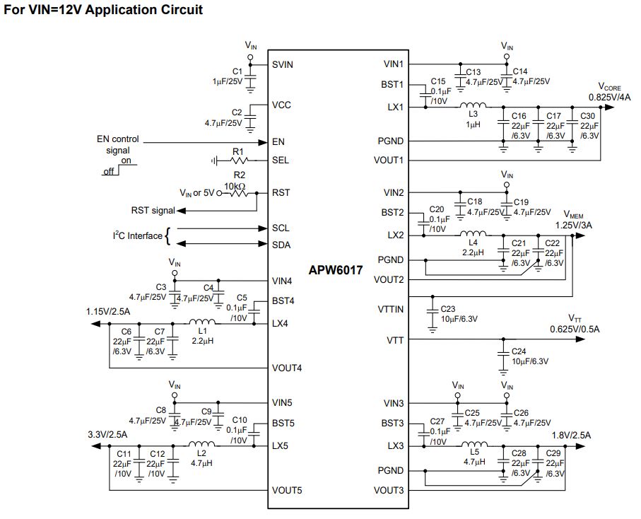
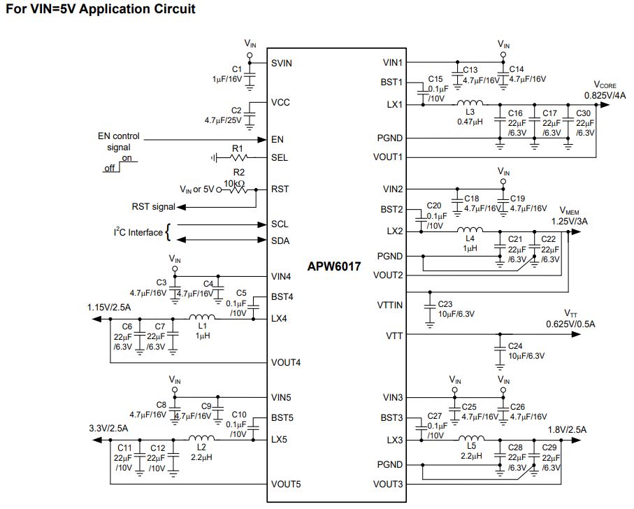
APW6017
Active
5 Buck Converters and 1 Termination LDO PMIC with I2C Interface
Features
- 4A output current capability
- 750KHz / 1.5MHz switching frequency
- 3A output current capability
- 750KHz / 1.5MHz switching frequency
- 2.5A output current capability
- 750KHz / 1.5MHz switching frequency
- 2.5A output current capability
- 750KHz / 1.5MHz switching frequency
- 2.5A output current capability
- 750KHz / 1.5MHz switching frequency
General Description
The APW6017 is designed for server management processor power system, which integrates 5 buck converters and one 0.5A sink/source VTT LDO into one single package. The PWM converters and VTT LDO output voltage can support VCORE, memory, memory bus termination and 1.8V/1.15V/3.3V I/O. Each VR voltage are programmable with high resolution via I2C interface. Moreover, the power-on and power-off sequences as well as soft-start time of these VR are controlled and programmable via I2C interface, providing versatility for system designers. The APW6017 provides excellent transient response and accurate DC voltage output in either PFM or PWM Mode. In Pulse Frequency Modulation mode (PFM), the APW6017 provides very high efficiency over light to heavy loads with loading-modulated switching frequencies. On VTQFN-32 Package, the Forced PWM Mode works nearly at constant frequency for low-noise requirements. The APW6017 features sufficient protections against over-current, over-voltage, short circuit and over-temperature to prevent catastrophic failure. A Power-On-Reset function monitors the voltage on SVIN prevents wrong operation during power on. The output voltage of VTT automatically tracks the voltage of half VOUT2. The VTT output voltage is only requiring 10µF of ceramic output capacitance for stability and fast transient response.
Features
- High Input Voltages Range from 4.5V to 16V
- Built in Input Voltage UVLO threshold
- Built in VIN OVP
- Programmable power sequence control by I2C for all channel
- Provide 5 Single-Buck PWM Converter and 1 Termination LDO Regulator
- Channel 1 Synchronous Buck for VCORE (Default 0.825V)
- 4A output current capability
- 750KHz / 1.5MHz switching frequency
- Channel 2 Synchronous Buck for Memory (Default 1.15V / 1.25V)
- 3A output current capability
- 750KHz / 1.5MHz switching frequency
- Channel 3 Synchronous Buck for I/O (Default 1.8V)
- 2.5A output current capability
- 750KHz / 1.5MHz switching frequency
- Channel 4 Synchronous Buck for I/O (Default 1.15V)
- 2.5A output current capability
- 750KHz / 1.5MHz switching frequency
- Channel 5 Synchronous Buck for I/O (Default 3.3V)
- 2.5A output current capability
- 750KHz / 1.5MHz switching frequency
- Channel 6 VTT Termination LDO Regulator
- Built-in EN function
- Built-in RST to monitor output voltage status
- Built-in Current Limit/SCP/OVP/OTP
- VTQFN-32 4mmx4mm Thin package
General Description
The APW6017 is designed for server management processor power system, which integrates 5 buck converters and one 0.5A sink/source VTT LDO into one single package. The PWM converters and VTT LDO output voltage can support VCORE, memory, memory bus termination and 1.8V/1.15V/3.3V I/O. Each VR voltage are programmable with high resolution via I2C interface. Moreover, the power-on and power-off sequences as well as soft-start time of these VR are controlled and programmable via I2C interface, providing versatility for system designers. The APW6017 provides excellent transient response and accurate DC voltage output in either PFM or PWM Mode. In Pulse Frequency Modulation mode (PFM), the APW6017 provides very high efficiency over light to heavy loads with loading-modulated switching frequencies. On VTQFN-32 Package, the Forced PWM Mode works nearly at constant frequency for low-noise requirements. The APW6017 features sufficient protections against over-current, over-voltage, short circuit and over-temperature to prevent catastrophic failure. A Power-On-Reset function monitors the voltage on SVIN prevents wrong operation during power on. The output voltage of VTT automatically tracks the voltage of half VOUT2. The VTT output voltage is only requiring 10µF of ceramic output capacitance for stability and fast transient response.
APW6017A
Active
5 Buck Converters and 1 Termination LDO PMIC with I2C Interface
Features
- 4A Output Current Capability
- 750kHz / 1.5MHz Switching Frequency
- 3A Output Current Capability
- 750kHz / 1.5MHz Switching Frequency
- 2.5A Output Current Capability
- 750kHz / 1.5MHz Switching Frequency
- 2.5A Output Current Capability
- 750kHz / 1.5MHz Switching Frequency
- 2.5A Output Current Capability
- 750kHz / 1.5MHz Switching Frequency
General Description
The APW6017A is designed for server management processor power system, which integrates 5 buck converters and one 0.5A sink/source VTT LDO into one single package. The PWM converters and VTT LDO output voltage can support VCORE, memory, memory bus termination and 1.8V/1.15V/3.3V I/O. Each VR voltage are programmable with high resolution via I2C interface. Moreover, the power-on and power-off sequences as well as soft-start time of these VR are controlled and programmable via I2C interface, providing versatility for system designers. The APW6017A provides excellent transient response and accurate DC voltage output in either PFM or PWM Mode. In Pulse Frequency Modulation mode (PFM), the APW6017A provides very high efficiency over light to heavy loads with loading-modulated switching frequencies. On VTQFN-32 Package, the Forced PWM Mode works nearly at constant frequency for low-noise requirements. The APW6017A features sufficient protections against over-current, over-voltage, short circuit and over temperature to prevent catastrophic failure. A Power-On-Reset function monitors the voltage on SVIN prevents wrong operation during power on. The output voltage of VTT automatically tracks the voltage of half VOUT2. The VTT output voltage is only requiring 10µF of ceramic output capacitance for stability and fast transient response.
Features
- High Input Voltages Range from 4.5V to 16V
- Built In Input Voltage UVLO Threshold
- Built In VIN OVP
- Programmable Power Sequence Control by I2C for all Channel
- Provide 5 Single-Buck PWM Converter and 1 Termination LDO Regulator
- Channel 1 Synchronous Buck for VCORE (Default 0.8V)
- 4A Output Current Capability
- 750kHz / 1.5MHz Switching Frequency
- Channel 2 Synchronous Buck for Memory (Default 1.1V / 1.2V)
- 3A Output Current Capability
- 750kHz / 1.5MHz Switching Frequency
- Channel 3 Synchronous Buck for I/O (Default 1.8V)
- 2.5A Output Current Capability
- 750kHz / 1.5MHz Switching Frequency
- Channel 4 Synchronous Buck for I/O (Default 1.15V)
- 2.5A Output Current Capability
- 750kHz / 1.5MHz Switching Frequency
- Channel 5 Synchronous Buck for I/O (Default 3.3V)
- 2.5A Output Current Capability
- 750kHz / 1.5MHz Switching Frequency
- Channel 6 VTT Termination LDO Regulator
- Built-In EN Function
- Built-In RST to Monitor Output Voltage Status
- Built-In Current Limit/SCP/OVP/OTP
- VTQFN-32 4mm x 4mm Thin Package
General Description
The APW6017A is designed for server management processor power system, which integrates 5 buck converters and one 0.5A sink/source VTT LDO into one single package. The PWM converters and VTT LDO output voltage can support VCORE, memory, memory bus termination and 1.8V/1.15V/3.3V I/O. Each VR voltage are programmable with high resolution via I2C interface. Moreover, the power-on and power-off sequences as well as soft-start time of these VR are controlled and programmable via I2C interface, providing versatility for system designers. The APW6017A provides excellent transient response and accurate DC voltage output in either PFM or PWM Mode. In Pulse Frequency Modulation mode (PFM), the APW6017A provides very high efficiency over light to heavy loads with loading-modulated switching frequencies. On VTQFN-32 Package, the Forced PWM Mode works nearly at constant frequency for low-noise requirements. The APW6017A features sufficient protections against over-current, over-voltage, short circuit and over temperature to prevent catastrophic failure. A Power-On-Reset function monitors the voltage on SVIN prevents wrong operation during power on. The output voltage of VTT automatically tracks the voltage of half VOUT2. The VTT output voltage is only requiring 10µF of ceramic output capacitance for stability and fast transient response.
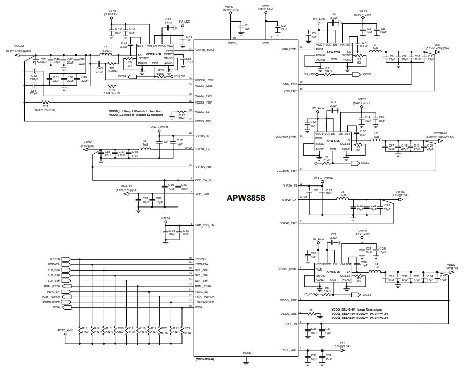
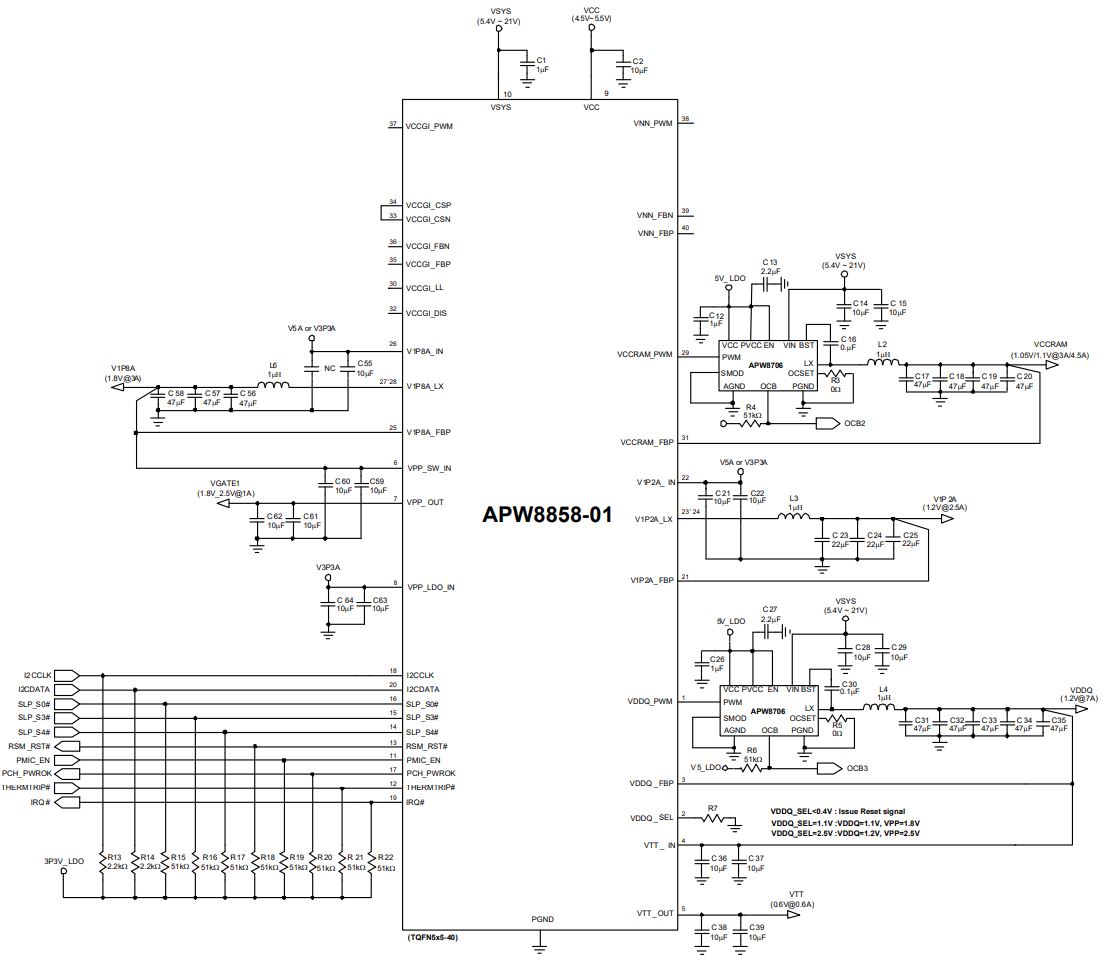
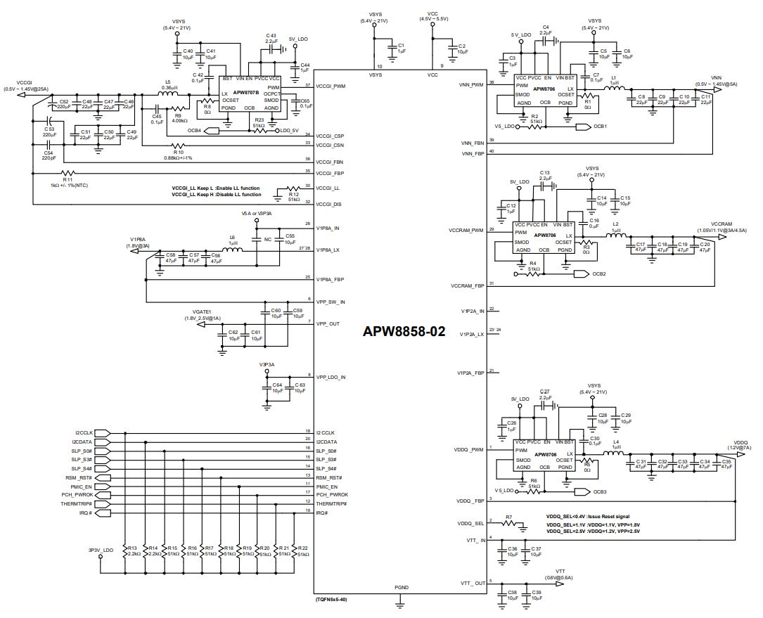
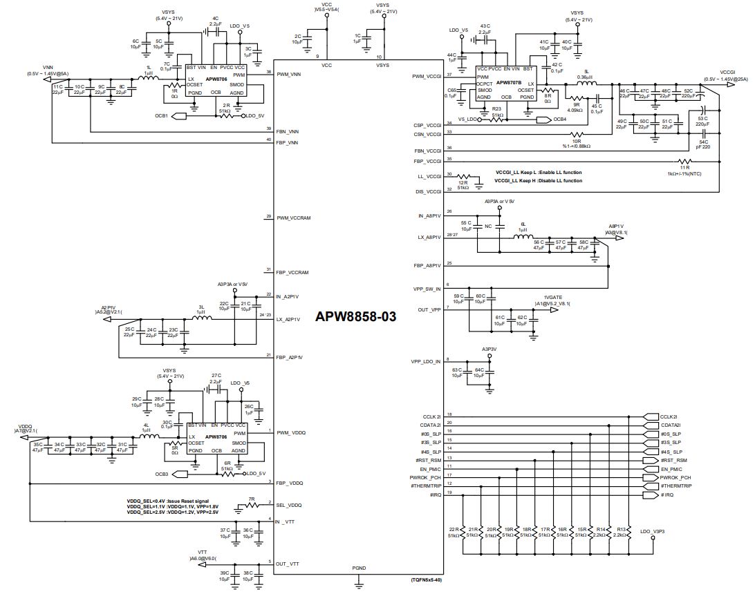
APW7276
Active
PMIC for LCD Bias Power
Features
- 13V/µs Slew Rate
- 10MHz, -3dB Bandwidth
General Description
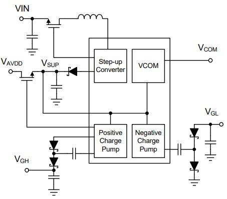
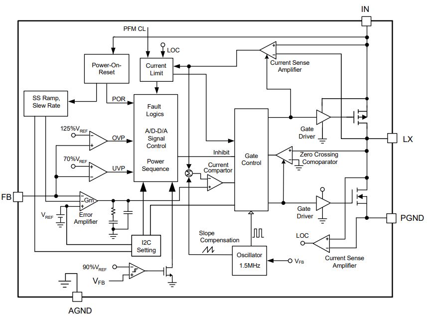
The APW7276 integrates with a high-performance step-up converter, two charge pump controllers and one high current operational amplifiers for TFT-LCD applications. The main step-up regulator is a current-mode, fixed-frequency PWM switching regulator. The 1.5MHz switching frequency allows the usage of low-profile inductors and ceramic capacitors to minimize the thickness of LCD panel designs. The charge pump controllers provide regulated the gate-driver of TFT-LCD VGH and VGL supplies. The amplifiers are ideal for VCOM applications, with 100mA output short circuit current drive, 10MHz bandwidth, and 13V/µs slew rate. All inputs and outputs are rail-to-rail. The APW7276 is available in a tiny 3mmx3mm 20-pin QFN package (TQFN3x3-20).
Features
- Input Voltage Range from 2.7V to 5.5V
- Positive & Negative Charge Pump for VGH & VGL
- High Performance Operation Amplifier
- 13V/µs Slew Rate
- 10MHz, -3dB Bandwidth
- Control Output for External P-MOSFET to Support Completely Disconnecting the Battery
- Adjustable Power Sequence by External Capacitor
- Internal Soft-start
- Cycle By Cycle Current Limit
- Multiple Overload Protection
- Over-Temperature Protection
- Available in TQFN3x3-20 Package
- Halogen and Lead Free Available (RoHS Compliant)
General Description
The APW7276 integrates with a high-performance step-up converter, two charge pump controllers and one high current operational amplifiers for TFT-LCD applications. The main step-up regulator is a current-mode, fixed-frequency PWM switching regulator. The 1.5MHz switching frequency allows the usage of low-profile inductors and ceramic capacitors to minimize the thickness of LCD panel designs. The charge pump controllers provide regulated the gate-driver of TFT-LCD VGH and VGL supplies. The amplifiers are ideal for VCOM applications, with 100mA output short circuit current drive, 10MHz bandwidth, and 13V/µs slew rate. All inputs and outputs are rail-to-rail. The APW7276 is available in a tiny 3mmx3mm 20-pin QFN package (TQFN3x3-20).
APW7279
Active
PMIC for LED BL + LCD Bias Power
Features
- Fast Transient Response
- 18V/700mA, 1.5Ω Internal N-MOS
- 0.2V Feedback Voltage
- 18V/2A, 0.3Ω internal N-MOS
General Description
The APW7279 integrates with two high-performance step-up converter and two charge pump controllers for TFTLCD and Backlight applications. Both the two step-up regulators are a current-mode, fixed-frequency PWM switching regulator. The 1.0MHz switching frequency allows the usage of low-profile inductors and ceramic capacitors to minimize the thickness of LCD panel designs. The charge pump controllers provide regulated the gatedriver of TFT-LCD VGH and VGL supplies. The APW7279 is available in a tiny 3mm x 3mm 20-pin TQFN package (TQFN3x3-20).
Features
- 2.9V to 5.5V Input Supply Range
- Current Mode Step-up Regulator (LCD bias)
- Fast Transient Response
- 18V/700mA, 1.5Ω Internal N-MOS
- Positive & Negative Charge Pump Driver for VGH, VGL
- Current Mode Step-up Regulator (LED BL)
- 0.2V Feedback Voltage
- 18V/2A, 0.3Ω internal N-MOS
- Control Output for External P-MOS to Support
- Completely Disconnecting the Battery
- Adjustable Power Sequencing by External Capacitor
- Internal Soft-Start
- Multiple Overload Protection
- Thermal Shutdown
- Available in Small Package : TQFN3x3-20
General Description
The APW7279 integrates with two high-performance step-up converter and two charge pump controllers for TFTLCD and Backlight applications. Both the two step-up regulators are a current-mode, fixed-frequency PWM switching regulator. The 1.0MHz switching frequency allows the usage of low-profile inductors and ceramic capacitors to minimize the thickness of LCD panel designs. The charge pump controllers provide regulated the gatedriver of TFT-LCD VGH and VGL supplies. The APW7279 is available in a tiny 3mm x 3mm 20-pin TQFN package (TQFN3x3-20).
APW7703A
Active
2.4MHz PMIC for Battery Powered System with I2C Controller
Features
Charger
- Programmable Input Current Limit: 100mA, 500mA, 900mA, 1300mA, 1700mA, 2100mA, 2500mA
- Battery Charge Preconditioning
- Charge Termination and Recharge
- ±7% Charge Current Regulation
- ±7.5% Input Current Regulation
- Thermal Shutdown
- Input Over-Voltage Protection
- MOSFET Over-Current Protection
Voltage Rail
- DC2: 0.6V - 3.3V at 1.5A
- DC3: 0.6V - 3.3V at 1A
- DC4: 0.6V - 3.3V at 1.5A
- LDO1 0.6V - 3.3V, 150mA, Reference=0.6V
- LDO2 1.5V - 3.05V, 300mA, Controlled by I2C
General Description
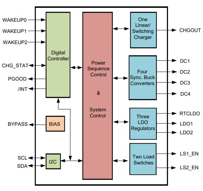
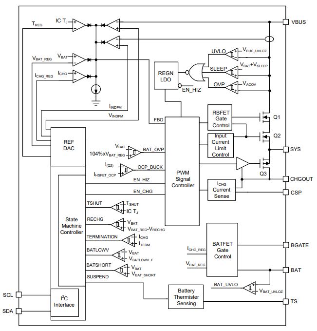
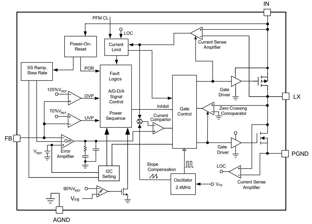
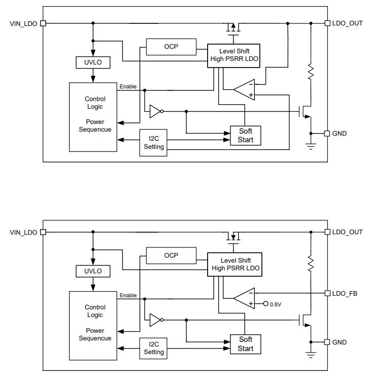
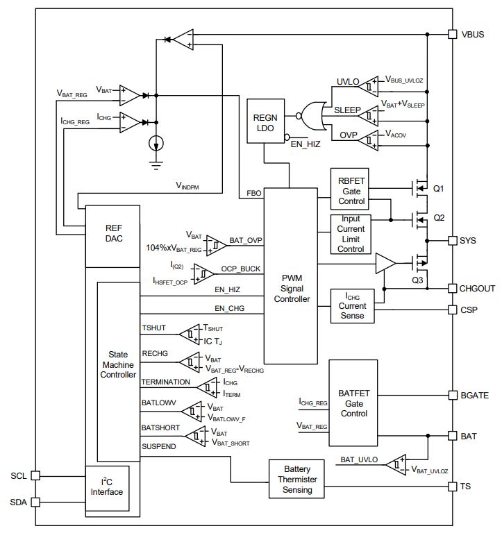
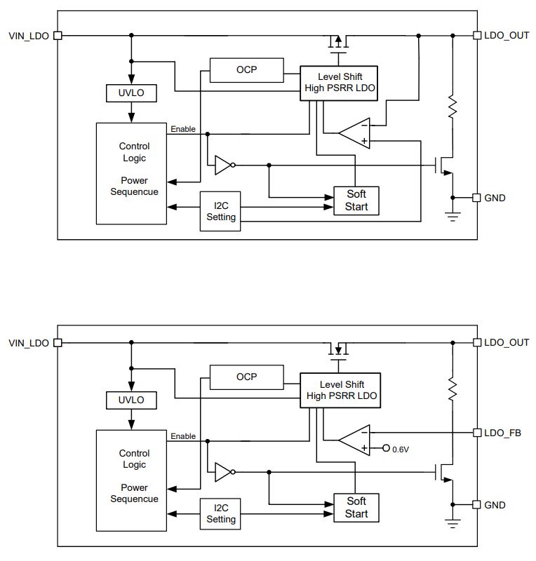
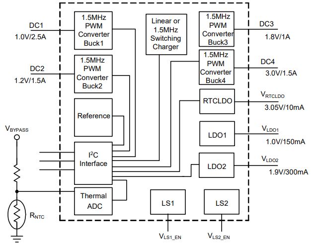
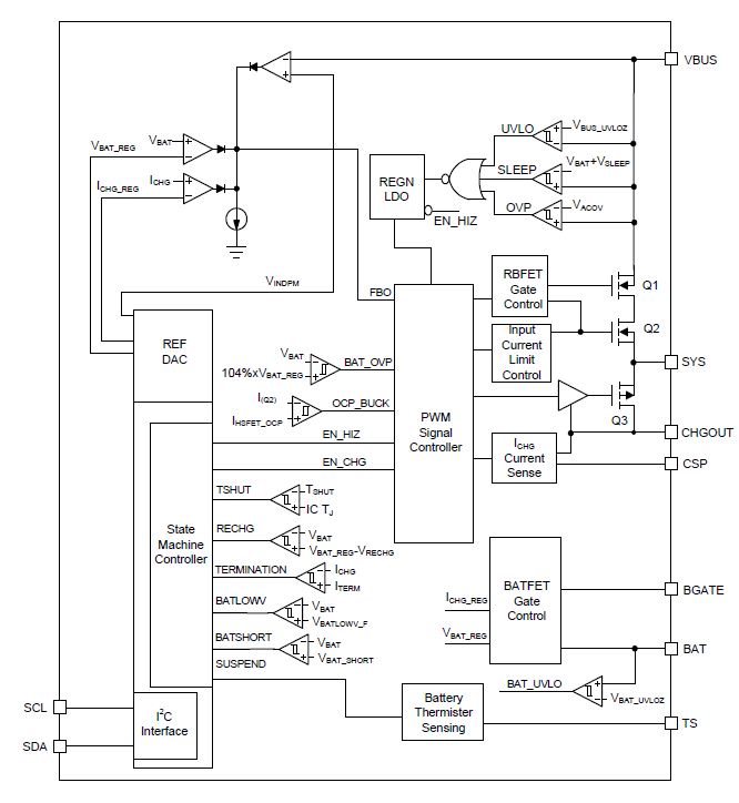
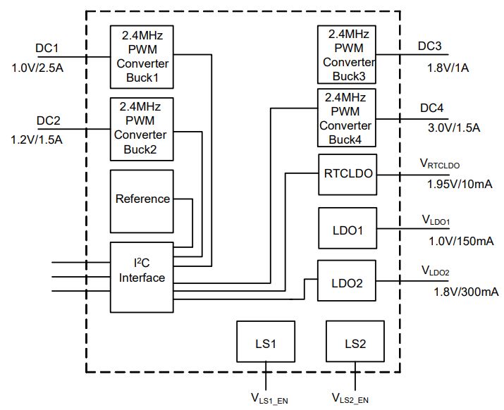
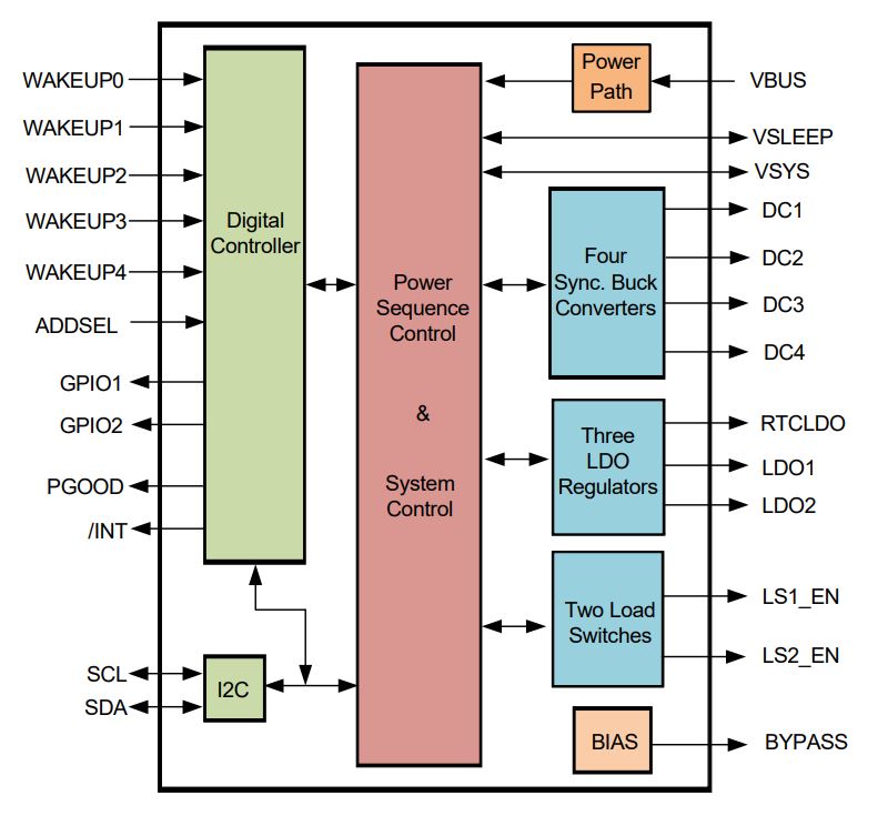
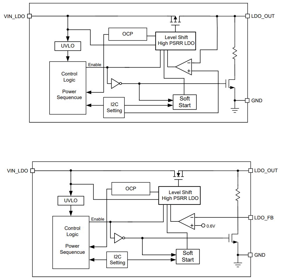
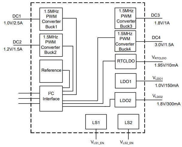
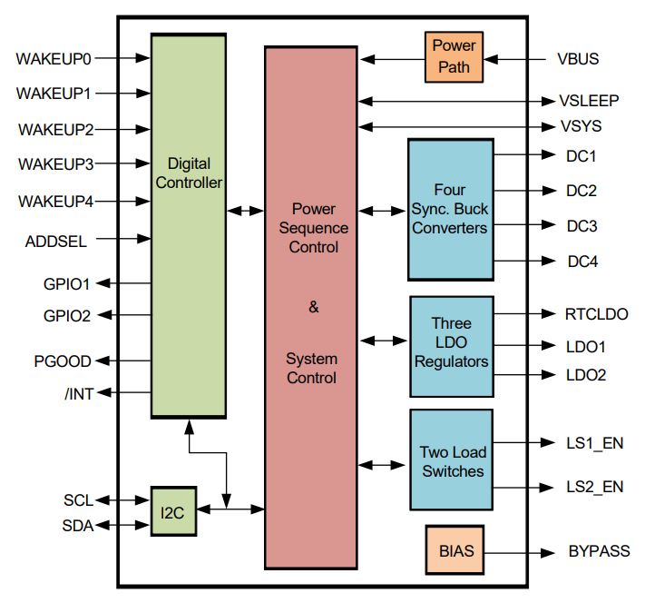
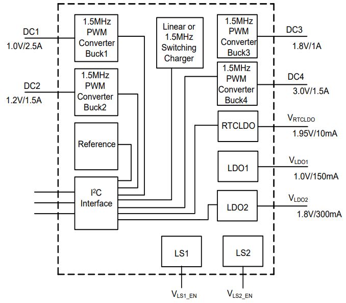
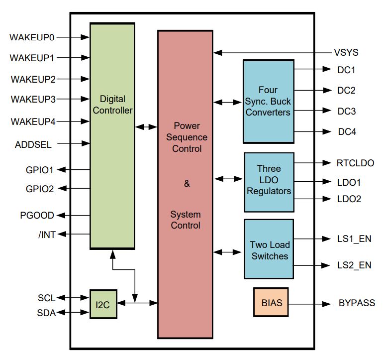
The APW7703A is a Power Management IC (PMIC) with a battery powered system designed to provide complete Power Management solution for the camera applications. The IC operates from a single supply voltage of 2.7V to 5.5V allowing it to be used in Adapter/USB or 1 Cell battery applications. The APW7703A is designed to provide maximum number of regulators in the smallest available cost effective package. Included in the IC are: One selectable linear mode or switch mode charger; Four switching Buck converters for DC1/DC2/DC3/DC4, Three LDOs for Image Signal Process and RTC applications, and Two Load Switch Enable Signal Control for Wi-Fi, DRAM applications. For Charger part, when the input current limit or voltage limit is reached, the power path management automatically reduces the charge current to zero. As the system load continues to increase, the power path discharges the battery until the system power requirement is met. This supplement mode operation prevents overloading the input source. The devices initiate and complete a charging cycle without software control. It automatically detects the battery voltage and charges the battery in three phases: pre-conditioning, constant current and constant voltage. At the end of the charging cycle, the charger automatically terminates when the charge current is below a preset limit in the constant voltage phase. When the full battery falls below the recharge threshold, the charger will automatically start another charging cycle. The device provides various safety features for battery charging operation, including a pack negative thermistor monitoring, charging safety timer and over-voltage/over-current protections. For the other VRs, the IC is equipped with all the standard protection features such as current limit, over voltage and internal under voltage lock out protection as well as thermal shutdown. The serial interface is an I2C communication interface which allows supply sequencing as well as controlled margining of ramp up and ramp down of all supplies to optimize battery power consumption. The I2C interface also allows for adjustability of VRs’ voltage and Forced PWM Mode in default operation and Auto PSM/PWM Mode in OFF mode state. Also, the power sequenc is defined by strobes and delay times under I2C Control. The device is available in a 40-pin, 5x5 mm2 thin QFN package for best thermal performance while optimizing the cost.
Features
Charger
- Available in Linear Mode or Switch Mode Charge
- High Efficiency 1.5A at Switch Mode Charge
- Single Input USB-compliant/Adapter Charge
- Programmable Input Current Limit: 100mA, 500mA, 900mA, 1300mA, 1700mA, 2100mA, 2500mA
- 3.9V-6V Input Operating Voltage Range
- 1.5MHz Switching Frequency for Low Profile Inductor
- Autonomous Battery Charging with or without Host Management
- Battery Charge Preconditioning
- Charge Termination and Recharge
- High Accuracy
- ±7% Charge Current Regulation
- ±7.5% Input Current Regulation
- Safety
- Thermal Shutdown
- Input Over-Voltage Protection
- MOSFET Over-Current Protection
Voltage Rail
- Provide 4 Buck Single Phase PWM Converters
- DC2: 0.6V - 3.3V at 1.5A
- DC3: 0.6V - 3.3V at 1A
- DC4: 0.6V - 3.3V at 1.5A
- Provide 3 LDO Output
- LDO1 0.6V - 3.3V, 150mA, Reference=0.6V
- LDO2 1.5V - 3.05V, 300mA, Controlled by I2C
- Provide 2 Load Switches Enable Signal
- 30µA Low Battery Leakage Current
- TQFN 5x5-40A Package
- Lead Free and Green Devices Available (RoHS Compliant)
General Description
The APW7703A is a Power Management IC (PMIC) with a battery powered system designed to provide complete Power Management solution for the camera applications. The IC operates from a single supply voltage of 2.7V to 5.5V allowing it to be used in Adapter/USB or 1 Cell battery applications. The APW7703A is designed to provide maximum number of regulators in the smallest available cost effective package. Included in the IC are: One selectable linear mode or switch mode charger; Four switching Buck converters for DC1/DC2/DC3/DC4, Three LDOs for Image Signal Process and RTC applications, and Two Load Switch Enable Signal Control for Wi-Fi, DRAM applications. For Charger part, when the input current limit or voltage limit is reached, the power path management automatically reduces the charge current to zero. As the system load continues to increase, the power path discharges the battery until the system power requirement is met. This supplement mode operation prevents overloading the input source. The devices initiate and complete a charging cycle without software control. It automatically detects the battery voltage and charges the battery in three phases: pre-conditioning, constant current and constant voltage. At the end of the charging cycle, the charger automatically terminates when the charge current is below a preset limit in the constant voltage phase. When the full battery falls below the recharge threshold, the charger will automatically start another charging cycle. The device provides various safety features for battery charging operation, including a pack negative thermistor monitoring, charging safety timer and over-voltage/over-current protections. For the other VRs, the IC is equipped with all the standard protection features such as current limit, over voltage and internal under voltage lock out protection as well as thermal shutdown. The serial interface is an I2C communication interface which allows supply sequencing as well as controlled margining of ramp up and ramp down of all supplies to optimize battery power consumption. The I2C interface also allows for adjustability of VRs’ voltage and Forced PWM Mode in default operation and Auto PSM/PWM Mode in OFF mode state. Also, the power sequenc is defined by strobes and delay times under I2C Control. The device is available in a 40-pin, 5x5 mm2 thin QFN package for best thermal performance while optimizing the cost.
APW7703C
Active
1.5MHz PMIC for Battery Powered System with I2C Controller
Features
Charger
- Programmable Input Current Limit: 100mA, 500mA, 900mA, 1300mA, 1700mA, 2100mA, 2500mA
- Battery Charge Preconditioning
- Charge Termination and Recharge
- ±7% Charge Current Regulation
- ±7.5% Input Current Regulation
- Thermal Shutdown
- Input Over-Voltage Protection
- MOSFET Over-Current Protection
Voltage Rail
- DC2: 0.6V - 3.3V at 1.5A
- DC3: 0.6V - 3.3V at 1A
- DC4: 0.6V - 3.3V at 1.5A
- LDO1 0.6V - 3.3V, 150mA, Reference=0.6V
- LDO2 1.5V - 3.05V, 300mA, Controlled by I2C
General Description
The APW7703C is a Power Management IC (PMIC) with a battery powered system designed to provide complete Power Management solution for the camera applications. The IC operates from a single supply voltage of 2.7V to 5.5V allowing it to be used in Adapter/USB or 1 Cell battery applications. The APW7703C is designed to provide maximum number of regulators in the smallest available cost effective package. Included in the IC are: One selectable linear mode or switch mode charger; Four switching Buck converters for DC1/DC2/DC3/DC4, Three LDOs for Image Signal Process and RTC applications, and Two Load Switch Enable Signal Control for Wi-Fi, DRAM applications. For Charger part, when the input current limit or voltage limit is reached, the power path management automatically reduces the charge current to zero. As the system load continues to increase, the power path discharges the battery until the system power requirement is met. This supplement mode operation prevents overloading the input source. The devices initiate and complete a charging cycle without software control. It automatically detects the battery voltage and charges the battery in three phases: pre-conditioning, constant current and constant voltage. At the end of the charging cycle, the charger automatically terminates when the charge current is below a preset limit in the constant voltage phase. When the full battery falls below the recharge threshold, the charger will automatically start another charging cycle. The device provides various safety features for battery charging operation, including a pack negative thermistor monitoring, charging safety timer and over-voltage/over-current protections. For the other VRs, the IC is equipped with all the standard protection features such as current limit, over voltage and internal under voltage lock out protection as well as thermal shutdown. The serial interface is an I2C communication interface which allows supply sequencing as well as controlled margining of ramp up and ramp down of all supplies to optimize battery power consumption. The I2C interface also allows for adjustability of VRs’ voltage and Forced PWM Mode in default operation and Auto PSM/PWM Mode in OFF mode state. Also, the power sequenc is defined by strobes and delay times under I2C Control. The device is available in a 40-pin, 5x5 mm2 thin QFN package for best thermal performance while optimizing the cost.
Features
Charger
- Available in Linear Mode or Switch Mode Charge
- High Efficiency 1.5A at Switch Mode Charge
- Single Input USB-compliant/Adapter Charge
- Programmable Input Current Limit: 100mA, 500mA, 900mA, 1300mA, 1700mA, 2100mA, 2500mA
- 4.0V-6V Input Operating Voltage Range
- 1.5MHz Switching Frequency for Low Profile Inductor
- Autonomous Battery Charging with or without Host Management
- Battery Charge Preconditioning
- Charge Termination and Recharge
- High Accuracy
- ±7% Charge Current Regulation
- ±7.5% Input Current Regulation
- Safety
- Thermal Shutdown
- Input Over-Voltage Protection
- MOSFET Over-Current Protection
Voltage Rail
- Provide 4 Buck Single Phase PWM Converters
- DC2: 0.6V - 3.3V at 1.5A
- DC3: 0.6V - 3.3V at 1A
- DC4: 0.6V - 3.3V at 1.5A
- Provide 3 LDO Output
- LDO1 0.6V - 3.3V, 150mA, Reference=0.6V
- LDO2 1.5V - 3.05V, 300mA, Controlled by I2C
- Provide 2 Load Switches Enable Signal
- 30µA Low Battery Leakage Current
- TQFN 5x5-40A Package
- Lead Free and Green Devices Available (RoHS Compliant)
General Description
The APW7703C is a Power Management IC (PMIC) with a battery powered system designed to provide complete Power Management solution for the camera applications. The IC operates from a single supply voltage of 2.7V to 5.5V allowing it to be used in Adapter/USB or 1 Cell battery applications. The APW7703C is designed to provide maximum number of regulators in the smallest available cost effective package. Included in the IC are: One selectable linear mode or switch mode charger; Four switching Buck converters for DC1/DC2/DC3/DC4, Three LDOs for Image Signal Process and RTC applications, and Two Load Switch Enable Signal Control for Wi-Fi, DRAM applications. For Charger part, when the input current limit or voltage limit is reached, the power path management automatically reduces the charge current to zero. As the system load continues to increase, the power path discharges the battery until the system power requirement is met. This supplement mode operation prevents overloading the input source. The devices initiate and complete a charging cycle without software control. It automatically detects the battery voltage and charges the battery in three phases: pre-conditioning, constant current and constant voltage. At the end of the charging cycle, the charger automatically terminates when the charge current is below a preset limit in the constant voltage phase. When the full battery falls below the recharge threshold, the charger will automatically start another charging cycle. The device provides various safety features for battery charging operation, including a pack negative thermistor monitoring, charging safety timer and over-voltage/over-current protections. For the other VRs, the IC is equipped with all the standard protection features such as current limit, over voltage and internal under voltage lock out protection as well as thermal shutdown. The serial interface is an I2C communication interface which allows supply sequencing as well as controlled margining of ramp up and ramp down of all supplies to optimize battery power consumption. The I2C interface also allows for adjustability of VRs’ voltage and Forced PWM Mode in default operation and Auto PSM/PWM Mode in OFF mode state. Also, the power sequenc is defined by strobes and delay times under I2C Control. The device is available in a 40-pin, 5x5 mm2 thin QFN package for best thermal performance while optimizing the cost.

APW7703D
Active
1.5MHz PMIC for Battery Powered System with I2C Controller
Features
Charger
- Programmable Input Current Limit: 100mA, 500mA, 900mA, 1300mA, 1700mA, 2100mA, 2500mA
- Battery Charge Preconditioning
- Charge Termination and Recharge
- ±7% Charge Current Regulation
- ±7.5% Input Current Regulation
- Thermal Shutdown
- Input Over-Voltage Protection
- MOSFET Over-Current Protection
Voltage Rail
- DC2: 0.6V - 3.3V at 1.5A
- DC3: 0.6V - 3.3V at 1A
- DC4: 0.6V - 3.3V at 1.5A
- LDO1 0.6V - 3.3V, 150mA, Reference=0.6V
- LDO2 1.5V - 3.05V, 300mA, Controlled by I2C
General Description
The APW7703D is a Power Management IC (PMIC) with a battery powered system designed to provide complete Power Management solution for the camera applications. The IC operates from a single supply voltage of 2.7V to 5.5V allowing it to be used in Adapter/USB or 1 Cell battery applications. The APW7703D is designed to provide maximum number of regulators in the smallest available cost effective package. Included in the IC are: One selectable linear mode or switch mode charger; Four switching Buck converters for DC1/DC2/DC3/DC4, Three LDOs for Image Signal Process and RTC applications, and Two Load Switch Enable Signal Control for Wi-Fi, DRAM applications. For Charger part, when the input current limit or voltage limit is reached, the power path management automatically reduces the charge current to zero. As the system load continues to increase, the power path discharges the battery until the system power requirement is met. This supplement mode operation prevents overloading the input source. The devices initiate and complete a charging cycle without software control. It automatically detects the battery voltage and charges the battery in three phases: pre-conditioning, constant current and constant voltage. At the end of the charging cycle, the charger automatically terminates when the charge current is below a preset limit in the constant voltage phase. When the full battery falls below the recharge threshold, the charger will automatically start another charging cycle. The device provides various safety features for battery charging operation, including a pack negative thermistor monitoring, charging safety timer and over-voltage/over-current protections. For the other VRs, the IC is equipped with all the standard protection features such as current limit, over voltage and internal under voltage lock out protection as well as thermal shutdown. The serial interface is an I2C communication interface which allows supply sequencing as well as controlled margining of ramp up and ramp down of all supplies to optimize battery power consumption. The I2C interface also allows for adjustability of VRs’ voltage and Forced PWM Mode in default operation and Auto PSM/PWM Mode in OFF mode state. Also, the power sequenc is defined by strobes and delay times under I2C Control. The device is available in a 40-pin, 5x5 mm2 thin QFN package for best thermal performance while optimizing the cost.
Features
Charger
- Available in Linear Mode or Switch Mode Charge
- High Efficiency 1.5A at Switch Mode Charge
- Single Input USB-compliant/Adapter Charge
- Programmable Input Current Limit: 100mA, 500mA, 900mA, 1300mA, 1700mA, 2100mA, 2500mA
- 3.9V-6V Input Operating Voltage Range
- 1.5MHz Switching Frequency for Low Profile Inductor
- Autonomous Battery Charging with or without Host Management
- Battery Charge Preconditioning
- Charge Termination and Recharge
- High Accuracy
- ±7% Charge Current Regulation
- ±7.5% Input Current Regulation
- Safety
- Thermal Shutdown
- Input Over-Voltage Protection
- MOSFET Over-Current Protection
Voltage Rail
- Provide 4 Buck Single Phase PWM Converters
- DC2: 0.6V - 3.3V at 1.5A
- DC3: 0.6V - 3.3V at 1A
- DC4: 0.6V - 3.3V at 1.5A
- Provide 3 LDO Output
- LDO1 0.6V - 3.3V, 150mA, Reference=0.6V
- LDO2 1.5V - 3.05V, 300mA, Controlled by I2C
- Provide 2 Load Switches Enable Signal
- 30µA Low Battery Leakage Current
- TQFN 5x5-40A Package
- Lead Free and Green Devices Available (RoHS Compliant)
General Description
The APW7703D is a Power Management IC (PMIC) with a battery powered system designed to provide complete Power Management solution for the camera applications. The IC operates from a single supply voltage of 2.7V to 5.5V allowing it to be used in Adapter/USB or 1 Cell battery applications. The APW7703D is designed to provide maximum number of regulators in the smallest available cost effective package. Included in the IC are: One selectable linear mode or switch mode charger; Four switching Buck converters for DC1/DC2/DC3/DC4, Three LDOs for Image Signal Process and RTC applications, and Two Load Switch Enable Signal Control for Wi-Fi, DRAM applications. For Charger part, when the input current limit or voltage limit is reached, the power path management automatically reduces the charge current to zero. As the system load continues to increase, the power path discharges the battery until the system power requirement is met. This supplement mode operation prevents overloading the input source. The devices initiate and complete a charging cycle without software control. It automatically detects the battery voltage and charges the battery in three phases: pre-conditioning, constant current and constant voltage. At the end of the charging cycle, the charger automatically terminates when the charge current is below a preset limit in the constant voltage phase. When the full battery falls below the recharge threshold, the charger will automatically start another charging cycle. The device provides various safety features for battery charging operation, including a pack negative thermistor monitoring, charging safety timer and over-voltage/over-current protections. For the other VRs, the IC is equipped with all the standard protection features such as current limit, over voltage and internal under voltage lock out protection as well as thermal shutdown. The serial interface is an I2C communication interface which allows supply sequencing as well as controlled margining of ramp up and ramp down of all supplies to optimize battery power consumption. The I2C interface also allows for adjustability of VRs’ voltage and Forced PWM Mode in default operation and Auto PSM/PWM Mode in OFF mode state. Also, the power sequenc is defined by strobes and delay times under I2C Control. The device is available in a 40-pin, 5x5 mm2 thin QFN package for best thermal performance while optimizing the cost.
APW7703E
Active
1.5MHz PMIC for Battery Powered System with I2C Controller
Features
Charger
- Programmable Input Current Limit: 100mA, 500mA, 900mA, 1300mA, 1700mA, 2100mA, 2500mA
- Battery Charge Preconditioning
- Charge Termination and Recharge
- ±7% Charge Current Regulation
- ±7.5% Input Current Regulation
- Thermal Shutdown
- Input Over-Voltage Protection
- MOSFET Over-Current Protection
Voltage Rail
- DC2: 0.6V - 3.3V at 1.5A
- DC3: 0.6V - 3.3V at 1A
- DC4: 0.6V - 3.3V at 2A
- LDO1 0.6V - 3.3V, 150mA, Reference=0.6V
- LDO2 1.5V - 3.05V, 300mA, Controlled by I2C
General Description
The APW7703E is a Power Management IC (PMIC) with a battery powered system designed to provide complete Power Management solution for the camera applications. The IC operates from a single supply voltage of 2.7V to 6.0V allowing it to be used in Adapter/USB or 1 Cell battery applications. The APW7703E is designed to provide maximum number of regulators in the smallest available cost effective package. Included in the IC are: One selectable linear mode or switch mode charger; Four switching Buck converters for DC1/DC2/DC3/DC4, Three LDOs for Image Signal Process and RTC applications. For Charger part, when the input current limit or voltage limit is reached, the power path management automatically reduces the charge current to zero. As the system load continues to increase, the power path discharges the battery until the system power requirement is met. This supplement mode operation prevents overloading the input source. The devices initiate and complete a charging cycle without software control. It automatically detects the battery voltage and charges the battery in three phases: pre-conditioning, constant current and constant voltage. At the end of the charging cycle, the charger automatically terminates when the charge current is below a preset limit in the constant voltage phase. When the full battery falls below the recharge threshold, the charger will automatically start another charging cycle. The device provides various safety features for battery charging operation, including a pack negative thermistor monitoring, charging safety timer and over-voltage/over-current protections. For the other VRs, the IC is equipped with all the standard protection features such as current limit, over voltage and internal voltage protection as well as thermal shutdown. The serial interface is an I2C communication interface which allows supply sequencing as well as controlled margining of ramp up and ramp down of all supplies to optimize battery power consumption. The I2C interface also allows for adjustability of VRs’ voltage and Forced PWM Mode in default operation and Auto PSM/PWM Mode in OFF mode state. Also, the power sequenc is defined by strobes and delay times under I2C Control. The device is available in a 40-pin, 5x5 mm2 thin QFN package for best thermal performance while optimizing the cost.
Features
Charger
- Available in Linear Mode or Switch Mode Charge
- High Efficiency 1.5A at Switch Mode Charge
- Single Input USB-compliant/Adapter Charge
- Programmable Input Current Limit: 100mA, 500mA, 900mA, 1300mA, 1700mA, 2100mA, 2500mA
- 4.0V-6V Input Operating Voltage Range
- 1.5MHz Switching Frequency for Low Profile Inductor
- Autonomous Battery Charging with or without Host Management
- Battery Charge Preconditioning
- Charge Termination and Recharge
- High Accuracy
- ±7% Charge Current Regulation
- ±7.5% Input Current Regulation
- Safety
- Thermal Shutdown
- Input Over-Voltage Protection
- MOSFET Over-Current Protection
Voltage Rail
- Provide 4 Buck Single Phase PWM Converters
- DC2: 0.6V - 3.3V at 1.5A
- DC3: 0.6V - 3.3V at 1A
- DC4: 0.6V - 3.3V at 2A
- Provide 3 LDO Output
- LDO1 0.6V - 3.3V, 150mA, Reference=0.6V
- LDO2 1.5V - 3.05V, 300mA, Controlled by I2C
- 30µA Low Battery Leakage Current
- TQFN 5x5-40A Package
General Description
The APW7703E is a Power Management IC (PMIC) with a battery powered system designed to provide complete Power Management solution for the camera applications. The IC operates from a single supply voltage of 2.7V to 6.0V allowing it to be used in Adapter/USB or 1 Cell battery applications. The APW7703E is designed to provide maximum number of regulators in the smallest available cost effective package. Included in the IC are: One selectable linear mode or switch mode charger; Four switching Buck converters for DC1/DC2/DC3/DC4, Three LDOs for Image Signal Process and RTC applications. For Charger part, when the input current limit or voltage limit is reached, the power path management automatically reduces the charge current to zero. As the system load continues to increase, the power path discharges the battery until the system power requirement is met. This supplement mode operation prevents overloading the input source. The devices initiate and complete a charging cycle without software control. It automatically detects the battery voltage and charges the battery in three phases: pre-conditioning, constant current and constant voltage. At the end of the charging cycle, the charger automatically terminates when the charge current is below a preset limit in the constant voltage phase. When the full battery falls below the recharge threshold, the charger will automatically start another charging cycle. The device provides various safety features for battery charging operation, including a pack negative thermistor monitoring, charging safety timer and over-voltage/over-current protections. For the other VRs, the IC is equipped with all the standard protection features such as current limit, over voltage and internal voltage protection as well as thermal shutdown. The serial interface is an I2C communication interface which allows supply sequencing as well as controlled margining of ramp up and ramp down of all supplies to optimize battery power consumption. The I2C interface also allows for adjustability of VRs’ voltage and Forced PWM Mode in default operation and Auto PSM/PWM Mode in OFF mode state. Also, the power sequenc is defined by strobes and delay times under I2C Control. The device is available in a 40-pin, 5x5 mm2 thin QFN package for best thermal performance while optimizing the cost.
APW7704
Active
2.4MHz PMIC for DVR with I2C Controller
Features
Voltage Rail
- DC2: 0.6V - 3.3V at 1.5A
- DC3: 0.6V - 3.3V at 1A
- DC4: 0.6V - 3.3V at 1.5A
- LDO1 0.6V-3.3V, 150mA, Reference=0.6V
- LDO2 1.5V-3.05V, 300mA, Controlled by I2C
General Description
The APW7704 is a Power Management IC (PMIC) designed to provide complete Power Management solution for the driving video recorder (DVR) applications. For the application, if the input power source supplies to VBUS terminal, the SLEEP pin short to ground is recommanded. Also, if the input source power supplies to the VSYS terminal, It’s recommended the SLEEP and VSYS Pinouts terminal are connected togather and the VBUS pin shorts to grond. The APW7704 is designed to provide maximum number of regulators in the smallest available cost effective package. Included in the IC are: Four Synchronous Buck Converters for DC1 ~ DC4; Three LDOs with one for RTC application, and Two Load Switch Enable Signal Control for external load switches application. For the Bucks, the IC is equipped with all the standard protection features such as current limit, over voltage and internal under voltage lock out protection as well as thermal shutdown. The serial interface is an I2C communication interface. The I2C interface also allows for adjustability of VRs’voltage. Also, the power sequenc is defined by strobes and delay times under I2C control. The device is available in a 40-pin, 5x5 mm2 thin QFN package for best thermal performance while optimizing the cost.
Features
Voltage Rail
- Provide 4 Buck Single Phase PWM Converters
- DC2: 0.6V - 3.3V at 1.5A
- DC3: 0.6V - 3.3V at 1A
- DC4: 0.6V - 3.3V at 1.5A
- Provide 3 LDO Output
- LDO1 0.6V-3.3V, 150mA, Reference=0.6V
- LDO2 1.5V-3.05V, 300mA, Controlled by I2C
- Provide 2 Load Switches Enable Signal
- Current Limit Protection
- Output Under-Voltage Protection
- Output Over-Voltage Protection
- Thermal Shutdown Protection
- TQFN 5x5-40A Package
- Lead Free and Green Devices Available (RoHS Compliant)
General Description
The APW7704 is a Power Management IC (PMIC) designed to provide complete Power Management solution for the driving video recorder (DVR) applications. For the application, if the input power source supplies to VBUS terminal, the SLEEP pin short to ground is recommanded. Also, if the input source power supplies to the VSYS terminal, It’s recommended the SLEEP and VSYS Pinouts terminal are connected togather and the VBUS pin shorts to grond. The APW7704 is designed to provide maximum number of regulators in the smallest available cost effective package. Included in the IC are: Four Synchronous Buck Converters for DC1 ~ DC4; Three LDOs with one for RTC application, and Two Load Switch Enable Signal Control for external load switches application. For the Bucks, the IC is equipped with all the standard protection features such as current limit, over voltage and internal under voltage lock out protection as well as thermal shutdown. The serial interface is an I2C communication interface. The I2C interface also allows for adjustability of VRs’voltage. Also, the power sequenc is defined by strobes and delay times under I2C control. The device is available in a 40-pin, 5x5 mm2 thin QFN package for best thermal performance while optimizing the cost.
APW7704A
Active
1.5MHz PMIC for DVR with I2C Controller
Features
Voltage Rail
- DC2: 0.6V - 3.3V at 1.5A
- DC3: 0.6V - 3.3V at 1A
- DC4: 0.6V - 3.3V at 1.5A
- LDO1 0.6V-3.3V, 150mA, Reference=0.6V
- LDO2 1.5V-3.05V, 300mA, Controlled by I2C
General Description
The APW7704A is a Power Management IC (PMIC) designed to provide complete Power Management solution for the driving video recorder (DVR) applications. For the application, if the input power source supplies to VBUS terminal, the SLEEP pin short to ground is recommanded. Also, if the input source power supplies to the VSYS terminal, It’s recommended the SLEEP and VSYS Pinouts terminal are connected togather and the VBUS pin shorts to grond. The APW7704A is designed to provide maximum number of regulators in the smallest available cost effective package. Included in the IC are: Four Synchronous Buck Converters for DC1 ~ DC4; Three LDOs with one for RTC application, and Two Load Switch Enable Signal Control for external load switches application. For the Bucks, the IC is equipped with all the standard protection features such as current limit, over voltage and internal under voltage lock out protection as well as thermal shutdown. The serial interface is an I2C communication interface. The I2C interface also allows for adjustability of VRs’ voltage. Also, the power sequenc is defined by strobes and delay times under I2C control. The device is available in a 40-pin, 5x5 mm2 thin QFN package for best thermal performance while optimizing the cost.
Features
Voltage Rail
- Provide 4 Buck Single Phase PWM Converters
- DC2: 0.6V - 3.3V at 1.5A
- DC3: 0.6V - 3.3V at 1A
- DC4: 0.6V - 3.3V at 1.5A
- Provide 3 LDO Output
- LDO1 0.6V-3.3V, 150mA, Reference=0.6V
- LDO2 1.5V-3.05V, 300mA, Controlled by I2C
- Provide 2 Load Switches Enable Signal
- Current Limit Protection
- Output Under-Voltage Protection
- Output Over-Voltage Protection
- Thermal Shutdown Protection
- TQFN 5x5-40A Package
- Lead Free and Green Devices Available (RoHS Compliant)
General Description
The APW7704A is a Power Management IC (PMIC) designed to provide complete Power Management solution for the driving video recorder (DVR) applications. For the application, if the input power source supplies to VBUS terminal, the SLEEP pin short to ground is recommanded. Also, if the input source power supplies to the VSYS terminal, It’s recommended the SLEEP and VSYS Pinouts terminal are connected togather and the VBUS pin shorts to grond. The APW7704A is designed to provide maximum number of regulators in the smallest available cost effective package. Included in the IC are: Four Synchronous Buck Converters for DC1 ~ DC4; Three LDOs with one for RTC application, and Two Load Switch Enable Signal Control for external load switches application. For the Bucks, the IC is equipped with all the standard protection features such as current limit, over voltage and internal under voltage lock out protection as well as thermal shutdown. The serial interface is an I2C communication interface. The I2C interface also allows for adjustability of VRs’ voltage. Also, the power sequenc is defined by strobes and delay times under I2C control. The device is available in a 40-pin, 5x5 mm2 thin QFN package for best thermal performance while optimizing the cost.
APW7704AH
Active
1.5MHz PMIC for DVR with I2C Controller
Features
Voltage Rail
- DC2: 0.6V - 3.3V at 1.5A
- DC3: 0.6V - 3.3V at 1A
- DC4: 0.6V - 3.3V at 1.5A
- LDO1 0.6V-3.3V, 150mA, Reference=0.6V
- LDO2 1.5V-3.05V, 300mA, Controlled by I2C
General Description
The APW7704AH is a Power Management IC (PMIC) designed to provide complete Power Management solution for the driving video recorder (DVR) applications. For the application, if the input power source supplies to VBUS terminal, the SLEEP pin short to ground is recommanded. Also, if the input source power supplies to the VSYS Terminal, It’s recommended the SLEEP and VSYS Pinouts terminal are connected togather and the VBUS pin shorts to grond. The APW7704AH is designed to provide maximum number of regulators in the smallest available cost effective package. Included in the IC are: Four Synchronous Buck Converters for DC1 ~ DC4; Three LDOs with one for RTC application, and Two Load Switch Enable Signal Control for external load switches application. For the Bucks, the IC is equipped with all the standard protection features such as current limit, over voltage and internal under voltage lock out protection as well as thermal shutdown. The serial interface is an I2C communication interface. The I2C interface also allows for adjustability of VRs’ voltage. Also, the power sequenc is defined by strobes and delay times under I2C Control. The device is available in a 40-pin, 5x5 mm2 thin QFN package for best thermal performance while optimizing the cost.
Features
Voltage Rail
- Provide 4 Buck Single Phase PWM Converters
- DC2: 0.6V - 3.3V at 1.5A
- DC3: 0.6V - 3.3V at 1A
- DC4: 0.6V - 3.3V at 1.5A
- Provide 3 LDO Output
- LDO1 0.6V-3.3V, 150mA, Reference=0.6V
- LDO2 1.5V-3.05V, 300mA, Controlled by I2C
- Provide 2 Load Switches Enable Signal
- Current Limit Protection
- Output Under-Voltage Protection
- Output Over-Voltage Protection
- Thermal Shutdown Protection
- TQFN 5x5-40A Package
- AEC-Q100 Qualified
- Lead Free and Green Devices Available (RoHS Compliant)
General Description
The APW7704AH is a Power Management IC (PMIC) designed to provide complete Power Management solution for the driving video recorder (DVR) applications. For the application, if the input power source supplies to VBUS terminal, the SLEEP pin short to ground is recommanded. Also, if the input source power supplies to the VSYS Terminal, It’s recommended the SLEEP and VSYS Pinouts terminal are connected togather and the VBUS pin shorts to grond. The APW7704AH is designed to provide maximum number of regulators in the smallest available cost effective package. Included in the IC are: Four Synchronous Buck Converters for DC1 ~ DC4; Three LDOs with one for RTC application, and Two Load Switch Enable Signal Control for external load switches application. For the Bucks, the IC is equipped with all the standard protection features such as current limit, over voltage and internal under voltage lock out protection as well as thermal shutdown. The serial interface is an I2C communication interface. The I2C interface also allows for adjustability of VRs’ voltage. Also, the power sequenc is defined by strobes and delay times under I2C Control. The device is available in a 40-pin, 5x5 mm2 thin QFN package for best thermal performance while optimizing the cost.
APW7704B
Active
1.5MHz PMIC for DVR with I2C Controller
Features
Voltage Rail
- DC2: 0.6V - 3.3V at 1.5A
- DC3: 0.6V - 3.3V at 1A
- DC4: 0.6V - 3.3V at 1.5A
- LDO1 0.6V - 3.3V, 150mA, Reference=0.6V
- LDO2 1.5V - 3.05V, 300mA, Controlled by I2C
General Description
The APW7704B is a Power Management IC (PMIC) designed to provide complete Power Management solution for the driving video recorder (DVR) applications. The APW7704B is designed to provide maximum number of regulators in the smallest available cost effective package. Included in the IC are: Four Synchronous Buck Converters for DC1 ~ DC4; Three LDOs with one for RTC application, and Two Load Switch Enable Signal Control for external load switches application. For the Bucks, the IC is equipped with all the standard protection features such as current limit, over voltage and internal under voltage lock out protection as well as thermal shutdown. The serial interface is an I2C communication interface. The I2C interface also allows for adjustability of VRs’voltage. Also, the power sequenc is defined by strobes and delay times under I2C control. The device is available in a 40-pin, 5x5 mm2 thin QFN package for best thermal performance while optimizing the cost.
Features
Voltage Rail
- Provide 4 Buck Single Phase PWM Converters
- DC2: 0.6V - 3.3V at 1.5A
- DC3: 0.6V - 3.3V at 1A
- DC4: 0.6V - 3.3V at 1.5A
- Provide 3 LDO Output
- LDO1 0.6V - 3.3V, 150mA, Reference=0.6V
- LDO2 1.5V - 3.05V, 300mA, Controlled by I2C
- Provide 2 Load Switches Enable Signal
- Current Limit Protection
- Output Under-Voltage Protection
- Output Over-Voltage Protection for Bucks
- Thermal Shutdown Protection
- TQFN 5x5-40B Package
- Lead Free and Green Devices Available (RoHS Compliant)
General Description
The APW7704B is a Power Management IC (PMIC) designed to provide complete Power Management solution for the driving video recorder (DVR) applications. The APW7704B is designed to provide maximum number of regulators in the smallest available cost effective package. Included in the IC are: Four Synchronous Buck Converters for DC1 ~ DC4; Three LDOs with one for RTC application, and Two Load Switch Enable Signal Control for external load switches application. For the Bucks, the IC is equipped with all the standard protection features such as current limit, over voltage and internal under voltage lock out protection as well as thermal shutdown. The serial interface is an I2C communication interface. The I2C interface also allows for adjustability of VRs’voltage. Also, the power sequenc is defined by strobes and delay times under I2C control. The device is available in a 40-pin, 5x5 mm2 thin QFN package for best thermal performance while optimizing the cost.
APW7704C
Active
1.5MHz PMIC for DVR with I2C Controller
Features
Voltage Rail
- DC2: 0.6V - 3.3V at 1.5A
- DC3: 0.6V - 3.3V at 1A
- DC4: 0.6V - 3.3V at 2A
- LDO1 0.6V - 3.3V, 150mA, Reference=0.6V
- LDO2 1.5V - 3.05V, 300mA, Controlled by I2C
General Description
The APW7704C is a Power Management IC (PMIC) designed to provide complete Power Management solution for the driving video recorder (DVR) applications. The APW7704C is designed to provide maximum number of regulators in the smallest available cost effective package. Included in the IC are: Four Synchronous Buck Converters for DC1 ~ DC4; Three LDOs with one for RTC application, and Two Load Switch Enable Signal Control for external load switches application. For the Bucks, the IC is equipped with all the standard protection features such as current limit, over voltage and internal under voltage protection as well as thermal shutdown. The serial interface is an I2C communication interface. The I2C interface also allows for adjustability of VRs’ voltage. Also, the power sequenc is defined by strobes and delay times under I2C control. The device is available in a 40-pin, 5x5 mm2 thin QFN package for best thermal performance while optimizing the cost.
Features
Voltage Rail
- Provide 4 Buck Single Phase PWM Converters
- DC2: 0.6V - 3.3V at 1.5A
- DC3: 0.6V - 3.3V at 1A
- DC4: 0.6V - 3.3V at 2A
- Provide 3 LDO Output
- LDO1 0.6V - 3.3V, 150mA, Reference=0.6V
- LDO2 1.5V - 3.05V, 300mA, Controlled by I2C
- Provide 2 Load Switches Enable Signal
- Current Limit Protection
- Output Under-Voltage Protection
- Output Over-Voltage Protection for Bucks
- Thermal Shutdown Protection
- TQFN 5x5-40B Package
General Description
The APW7704C is a Power Management IC (PMIC) designed to provide complete Power Management solution for the driving video recorder (DVR) applications. The APW7704C is designed to provide maximum number of regulators in the smallest available cost effective package. Included in the IC are: Four Synchronous Buck Converters for DC1 ~ DC4; Three LDOs with one for RTC application, and Two Load Switch Enable Signal Control for external load switches application. For the Bucks, the IC is equipped with all the standard protection features such as current limit, over voltage and internal under voltage protection as well as thermal shutdown. The serial interface is an I2C communication interface. The I2C interface also allows for adjustability of VRs’ voltage. Also, the power sequenc is defined by strobes and delay times under I2C control. The device is available in a 40-pin, 5x5 mm2 thin QFN package for best thermal performance while optimizing the cost.
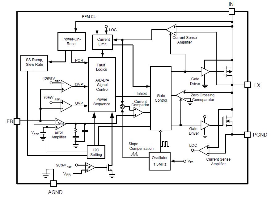
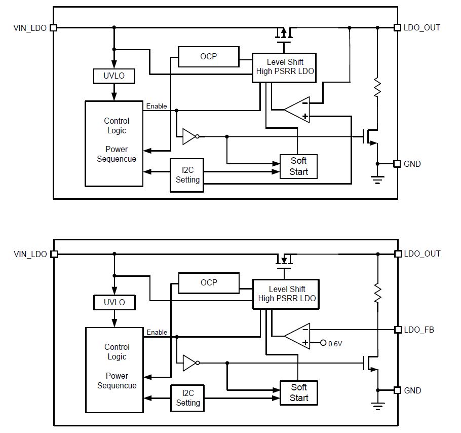
APW7704D
Active
1.5MHz PMIC for DVR with I2C Controller
Features
Voltage Rail
- DC2: 0.6V - 3.3V at 1.5A
- DC3: 0.6V - 3.3V at 1A
- DC4: 0.6V - 3.3V at 2A
- LDO1 0.6V - 3.3V, 150mA, Reference=0.6V
- LDO2 1.5V - 3.05V, 300mA, Controlled by I2C
General Description
The APW7704D is a Power Management IC (PMIC) designed to provide complete Power Management solution for the driving video recorder (DVR) applications. The APW7704D is designed to provide maximum number of regulators in the smallest available cost effective package. Included in the IC are: Four Synchronous Buck Converters for DC1 ~ DC4; Three LDOs with one for RTC application, and Two Load Switch Enable Signal Control for external load switches application. For the Bucks, the IC is equipped with all the standard protection features such as current limit, over voltage and internal under voltage lock out protection as well as thermal shutdown. The serial interface is an I2C communication interface. The I2C interface also allows for adjustability of VRs’voltage. Also, the power sequenc is defined by strobes and delay times under I2C control. The device is available in a 40-pin, 5x5 mm2 thin QFN package for best thermal performance while optimizing the cost.
Features
Voltage Rail
- Provide 4 Buck Single Phase PWM Converters
- DC2: 0.6V - 3.3V at 1.5A
- DC3: 0.6V - 3.3V at 1A
- DC4: 0.6V - 3.3V at 2A
- Provide 3 LDO Output
- LDO1 0.6V - 3.3V, 150mA, Reference=0.6V
- LDO2 1.5V - 3.05V, 300mA, Controlled by I2C
- Provide 2 Load Switches Enable Signal
- Current Limit Protection
- Output Under-Voltage Protection
- Output Over-Voltage Protection for Bucks
- Thermal Shutdown Protection
- TQFN 5x5-40B Package
- Lead Free and Green Devices Available (RoHS Compliant)
General Description
The APW7704D is a Power Management IC (PMIC) designed to provide complete Power Management solution for the driving video recorder (DVR) applications. The APW7704D is designed to provide maximum number of regulators in the smallest available cost effective package. Included in the IC are: Four Synchronous Buck Converters for DC1 ~ DC4; Three LDOs with one for RTC application, and Two Load Switch Enable Signal Control for external load switches application. For the Bucks, the IC is equipped with all the standard protection features such as current limit, over voltage and internal under voltage lock out protection as well as thermal shutdown. The serial interface is an I2C communication interface. The I2C interface also allows for adjustability of VRs’voltage. Also, the power sequenc is defined by strobes and delay times under I2C control. The device is available in a 40-pin, 5x5 mm2 thin QFN package for best thermal performance while optimizing the cost.
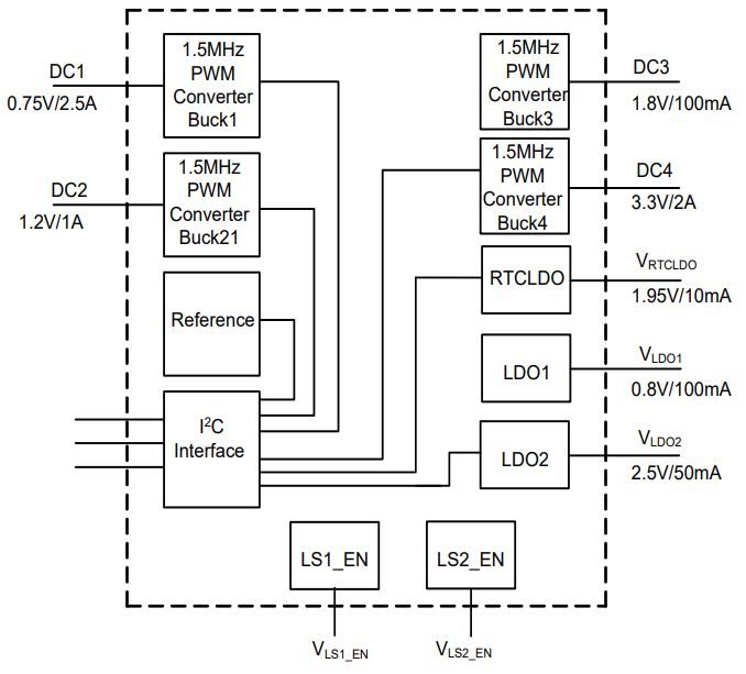
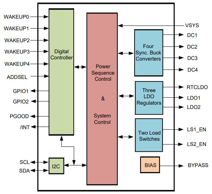
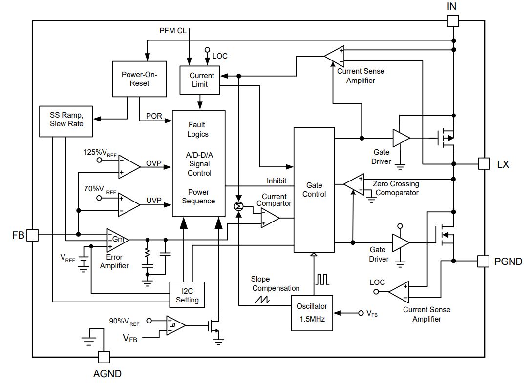
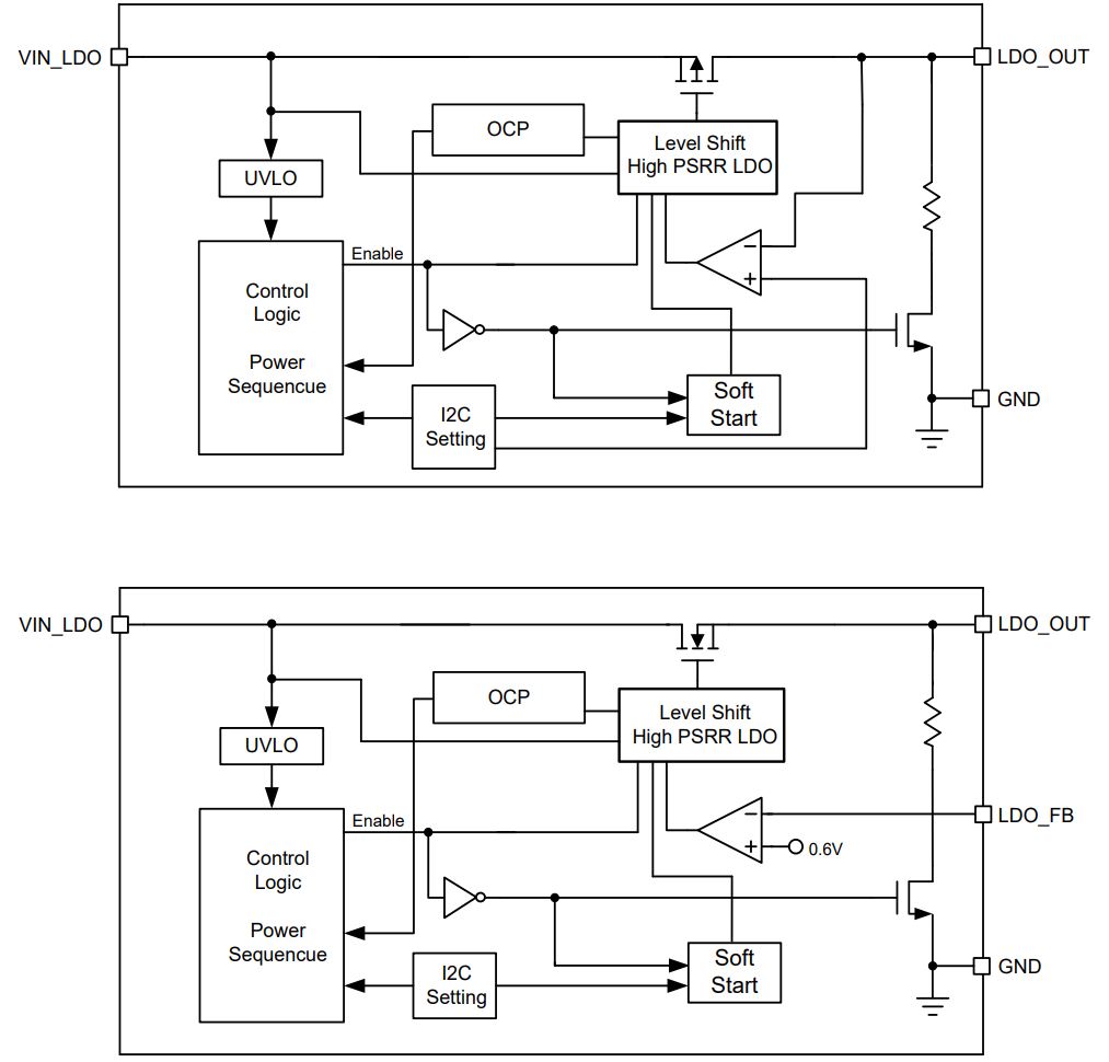
APW7704E
Active
1.5MHz PMIC for DVR with I2C Controller
Features
Voltage Rail
- DC2: 0.6V - 3.3V at 1.5A
- DC3: 0.6V - 3.3V at 1A
- DC4: 0.6V - 3.3V at 2A
- LDO1 0.6V - 3.3V, 150mA, Reference=0.6V
- LDO2 1.5V - 3.05V, 300mA, Controlled by I2C
General Description
The APW7704E is a Power Management IC (PMIC) designed to provide complete Power Management solution for the driving video recorder (DVR) applications. The APW7704E is designed to provide maximum number of regulators in the smallest available cost effective package. Included in the IC are: Four Synchronous Buck Converters for DC1 ~ DC4; Three LDOs with one for RTC application, and Two Load Switch Enable Signal Control for external load switches application. For the Bucks, the IC is equipped with all the standard protection features such as current limit, over voltage and internal under voltage lock out protection as well as thermal shutdown. The serial interface is an I2C communication interface. The I2C interface also allows for adjustability of VRs’voltage. Also, the power sequenc is defined by strobes and delay times under I2C Control. The device is available in a 40-pin, 5x5 mm2 thin QFN package for best thermal performance while optimizing the cost.
Features
Voltage Rail
- Provide 4 Buck Single Phase PWM Converters
- DC2: 0.6V - 3.3V at 1.5A
- DC3: 0.6V - 3.3V at 1A
- DC4: 0.6V - 3.3V at 2A
- Provide 3 LDO Output
- LDO1 0.6V - 3.3V, 150mA, Reference=0.6V
- LDO2 1.5V - 3.05V, 300mA, Controlled by I2C
- Provide 2 Load Switches Enable Signal
- Current Limit Protection
- Output Under-Voltage Protection
- Output Over-Voltage Protection for Bucks
- Thermal Shutdown Protection
- TQFN 5x5-40 Package
- Lead Free and Green Devices Available (RoHS Compliant)
General Description
The APW7704E is a Power Management IC (PMIC) designed to provide complete Power Management solution for the driving video recorder (DVR) applications. The APW7704E is designed to provide maximum number of regulators in the smallest available cost effective package. Included in the IC are: Four Synchronous Buck Converters for DC1 ~ DC4; Three LDOs with one for RTC application, and Two Load Switch Enable Signal Control for external load switches application. For the Bucks, the IC is equipped with all the standard protection features such as current limit, over voltage and internal under voltage lock out protection as well as thermal shutdown. The serial interface is an I2C communication interface. The I2C interface also allows for adjustability of VRs’voltage. Also, the power sequenc is defined by strobes and delay times under I2C Control. The device is available in a 40-pin, 5x5 mm2 thin QFN package for best thermal performance while optimizing the cost.
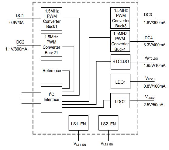
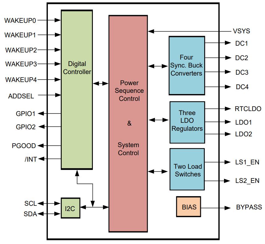
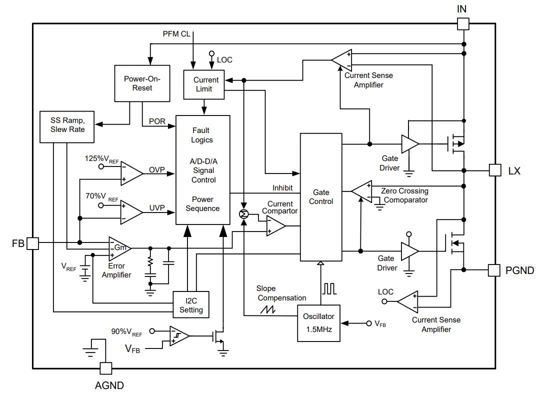
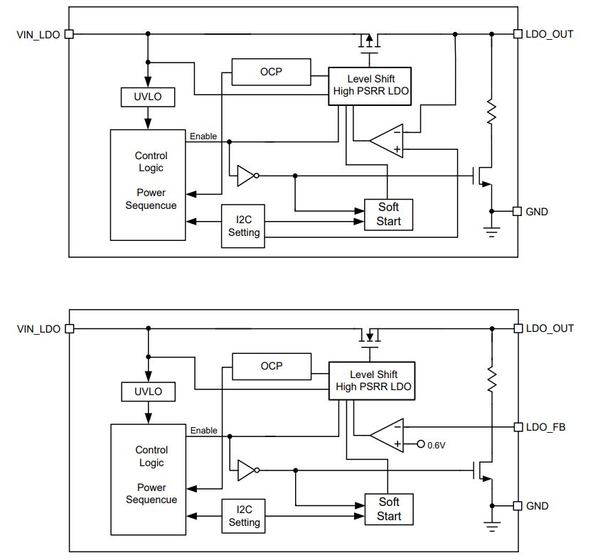
APW7704F
Active
1.5MHz PMIC for DVR with I2C Controller
Features
Voltage Rail
- DC2: 0.6V - 3.3V at 1.5A
- DC3: 0.6V - 3.3V at 1A
- DC4: 0.6V - 3.3V at 1.5A
- LDO1 0.6V - 3.3V, 150mA, Reference=0.6V
- LDO2 1.5V - 3.05V, 300mA, Controlled by I2C
General Description
The APW7704F is a Power Management IC (PMIC) designed to provide complete Power Management solution for the Human Machine Interface (HMI) applications. The APW7704F is designed to provide maximum number of regulators in the smallest available cost effective package. Included in the IC are: Four Synchronous Buck Converters for DC1 ~ DC4; Three LDOs with one for RTC application. For the Bucks, the IC is equipped with all the standard protection features such as current limit, over voltage and internal under voltage protection as well as thermal shutdown. The serial interface is an I2C communication interface. The I2C interface also allows for adjustability of VRs’ voltage. Also, the power sequenc is defined by strobes and delay times under I2C Control. The device is available in a 40-pin, 5x5 mm2 thin QFN package for best thermal performance while optimizing the cost.
Features
Voltage Rail
- Provide 4 Buck Single Phase PWM Converters
- DC2: 0.6V - 3.3V at 1.5A
- DC3: 0.6V - 3.3V at 1A
- DC4: 0.6V - 3.3V at 1.5A
- Provide 3 LDO Output
- LDO1 0.6V - 3.3V, 150mA, Reference=0.6V
- LDO2 1.5V - 3.05V, 300mA, Controlled by I2C
- Current Limit Protection
- Output Under-Voltage Protection
- Output Over-Voltage Protection for Bucks
- Thermal Shutdown Protection
- TQFN 5x5-40 Package
General Description
The APW7704F is a Power Management IC (PMIC) designed to provide complete Power Management solution for the Human Machine Interface (HMI) applications. The APW7704F is designed to provide maximum number of regulators in the smallest available cost effective package. Included in the IC are: Four Synchronous Buck Converters for DC1 ~ DC4; Three LDOs with one for RTC application. For the Bucks, the IC is equipped with all the standard protection features such as current limit, over voltage and internal under voltage protection as well as thermal shutdown. The serial interface is an I2C communication interface. The I2C interface also allows for adjustability of VRs’ voltage. Also, the power sequenc is defined by strobes and delay times under I2C Control. The device is available in a 40-pin, 5x5 mm2 thin QFN package for best thermal performance while optimizing the cost.
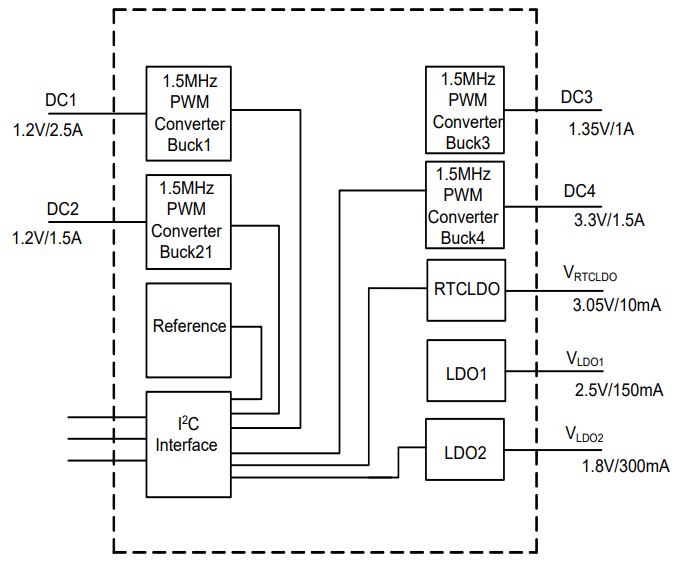
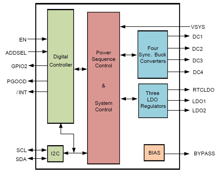
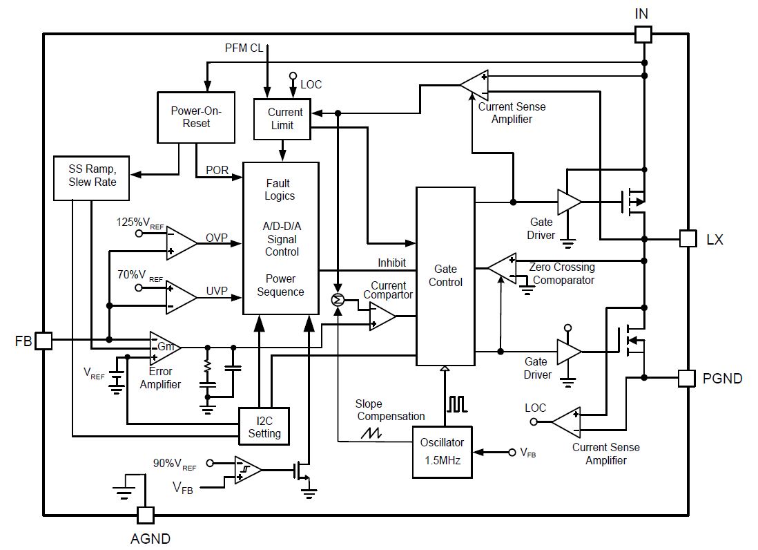
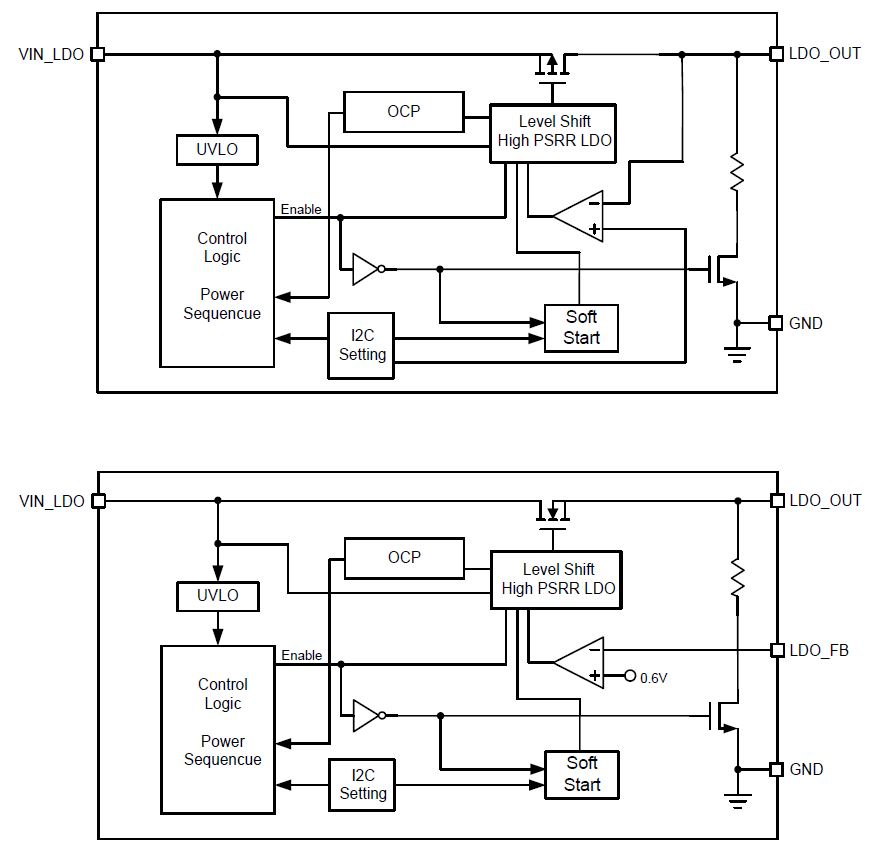
APW7708
Active
The PMIC with 4 Buck Converters, 3 LDOs, 2 Load Switches, and Flexible System Settings Via I2C Controller
Features
Voltage Rail
- DC2: 0.5V - 3.3V at 1.5A
- DC3: 0.6V - 3.3V at 1A
- DC4: 0.6V - 3.3V at 1.5A
- LDO1 0.6V - 3.3V, 150mA, Reference=0.6V
- LDO2 1.2V - 2.44V, 150mA, Controlled by I2C
General Description
The APW7708 is a Power Management IC (PMIC) designed to provide complete Power Management solution for the driving video recorder (DVR) applications. The APW7708 is designed to provide maximum number of regulators in the smallest available cost eff ective package. Included in the IC are: Four Synchronous Buck Converters for DC1 ~ DC4; Three LDOs with one for RTC application, and Two Load Switch Enable Signal Control for external load switches application. For the Bucks, the IC is equipped with all the standard protection features such as current limit, over voltage and internal under voltage protection as well as thermal shutdown. The serial interface is an I2C communication interface. The I2C interface also allows for adjustability of VRs’ voltage. Also, the power sequence is defi ned by strobes and delay times under I2C Control. The device is available in a 40-pin, 5x5 mm2 thin QFN package for best thermal performance while optimizing the cost.
Features
Voltage Rail
- Provide 4 Buck Single Phase PWM Converters
- DC2: 0.5V - 3.3V at 1.5A
- DC3: 0.6V - 3.3V at 1A
- DC4: 0.6V - 3.3V at 1.5A
- Provide 3 LDO Output
- LDO1 0.6V - 3.3V, 150mA, Reference=0.6V
- LDO2 1.2V - 2.44V, 150mA, Controlled by I2C
- Provide 2 Load Switches Enable Signal
- Current Limit Protection
- Output Under-Voltage Protection
- Output Over-Voltage Protection for Bucks
- Thermal Shutdown Protection
- TQFN 5x5-40A Package
General Description
The APW7708 is a Power Management IC (PMIC) designed to provide complete Power Management solution for the driving video recorder (DVR) applications. The APW7708 is designed to provide maximum number of regulators in the smallest available cost eff ective package. Included in the IC are: Four Synchronous Buck Converters for DC1 ~ DC4; Three LDOs with one for RTC application, and Two Load Switch Enable Signal Control for external load switches application. For the Bucks, the IC is equipped with all the standard protection features such as current limit, over voltage and internal under voltage protection as well as thermal shutdown. The serial interface is an I2C communication interface. The I2C interface also allows for adjustability of VRs’ voltage. Also, the power sequence is defi ned by strobes and delay times under I2C Control. The device is available in a 40-pin, 5x5 mm2 thin QFN package for best thermal performance while optimizing the cost.
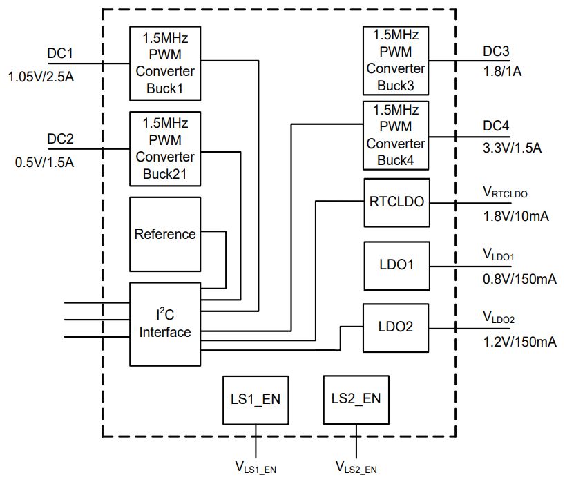
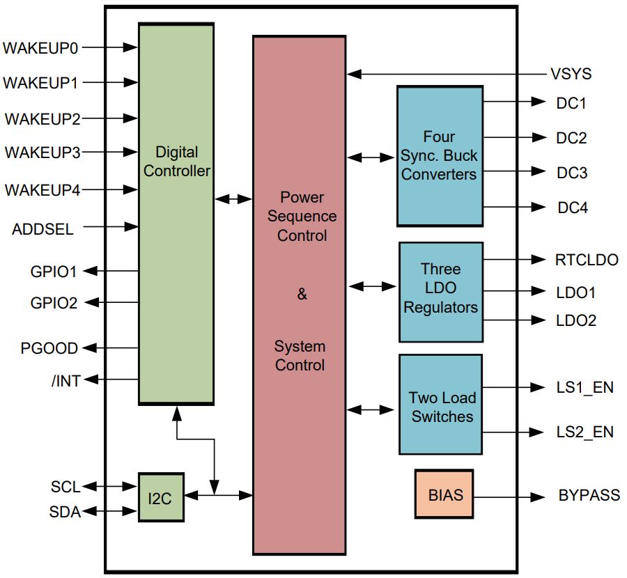
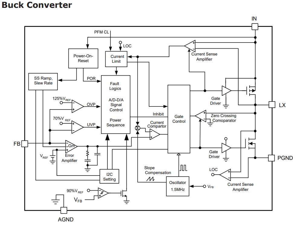
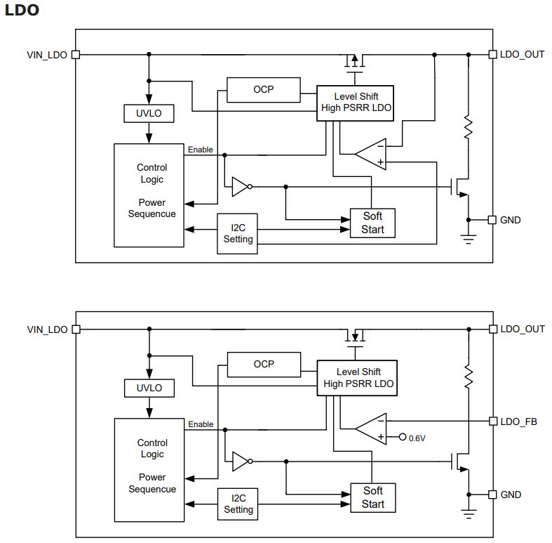
APW7713
Active
1.5MHz PMIC for Battery Powered System with I2C Controller
Features
Charger
- Programmable Input Current Limit: 100mA, 500mA, 900mA, 1300mA, 1700mA, 2100mA, 2500mA
- Battery Charge Preconditioning
- Charge Termination and Recharge
- ±7% Charge Current Regulation
- ±7.5% Input Current Regulation
- Thermal Shutdown
- Input Over-Voltage Protection
- MOSFET Over-Current Protection
Voltage Rail
- DC2: 0.6V - 3.3V at 1.5A
- DC3: 0.6V - 3.3V at 1A
- DC4: 0.6V - 3.3V at 2A
- LDO1 0.6V - 3.3V, 150mA, Reference=0.6V
- LDO2 1.5V - 3.05V, 300mA, Controlled by I2C
General Description
The APW7713 is a Power Management IC (PMIC) with a battery powered system designed to provide complete Power Management solution for the camera applications. The IC operates from a single supply voltage of 2.7V to 6.0V allowing it to be used in Adapter/USB or 1 Cell battery applications. The APW7713 is designed to provide maximum number of regulators in the smallest available cost effective package. Included in the IC are: One selectable linear mode or switch mode charger; Four switching Buck converters for DC1/DC2/DC3/DC4, Three LDOs for Image Signal Process and RTC applications, and Two Load Switch Enable Signal Control for Wi-Fi, DRAM applications. For Charger part, when the input current limit or voltage limit is reached, the power path management automatically reduces the charge current to zero. As the system load continues to increase, the power path discharges the battery until the system power requirement is met. This supplement mode operation prevents overloading the input source. The devices initiate and complete a charging cycle without software control. It automatically detects the battery voltage and charges the battery in three phases: pre-conditioning, constant current and constant voltage. At the end of the charging cycle, the charger automatically terminates when the charge current is below a preset limit in the constant voltage phase. When the full battery falls below the recharge threshold, the charger will automatically start another charging cycle. The device provides various safety features for battery charging operation, including a pack negative thermistor monitoring, charging safety timer and over-voltage/over-current protections. For the other VRs, the IC is equipped with all the standard protection features such as current limit, over voltage and internal under voltage lock out protection as well as thermal shutdown. The serial interface is an I2C communication interface which allows supply sequencing as well as controlled margining of ramp up and ramp down of all supplies to optimize battery power consumption. The I2C interface also allows for adjustability of VRs’ voltage and Forced PWM Mode in default operation and Auto PSM/PWM Mode in OFF mode state. Also, the power sequenc is defined by strobes and delay times under I2C Control. The device is available in a 40-pin, 5x5 mm2 thin QFN package for best thermal performance while optimizing the cost.
Features
Charger
- Available in Linear Mode or Switch Mode Charge
- High Efficiency 1.5A at Switch Mode Charge
- Single Input USB-compliant/Adapter Charge
- Programmable Input Current Limit: 100mA, 500mA, 900mA, 1300mA, 1700mA, 2100mA, 2500mA
- 4V-6V Input Operating Voltage Range
- 1.5MHz Switching Frequency for Low Profile Inductor
- Autonomous Battery Charging with or without Host Management
- Battery Charge Preconditioning
- Charge Termination and Recharge
- High Accuracy
- ±7% Charge Current Regulation
- ±7.5% Input Current Regulation
- Safety
- Thermal Shutdown
- Input Over-Voltage Protection
- MOSFET Over-Current Protection
Voltage Rail
- Provide 4 Buck Single Phase PWM Converters
- DC2: 0.6V - 3.3V at 1.5A
- DC3: 0.6V - 3.3V at 1A
- DC4: 0.6V - 3.3V at 2A
- Provide 3 LDO Output
- LDO1 0.6V - 3.3V, 150mA, Reference=0.6V
- LDO2 1.5V - 3.05V, 300mA, Controlled by I2C
- Provide 2 Load Switches Enable Signal
- 30µA Low Battery Leakage Current
- 1µA Low Battery Leakage Current in Shipping Mode
- Integrated ADC for System and Battery Monitor
- Always-On Push Bottom Monitor
- TQFN 5x5-40A Package
General Description
The APW7713 is a Power Management IC (PMIC) with a battery powered system designed to provide complete Power Management solution for the camera applications. The IC operates from a single supply voltage of 2.7V to 6.0V allowing it to be used in Adapter/USB or 1 Cell battery applications. The APW7713 is designed to provide maximum number of regulators in the smallest available cost effective package. Included in the IC are: One selectable linear mode or switch mode charger; Four switching Buck converters for DC1/DC2/DC3/DC4, Three LDOs for Image Signal Process and RTC applications, and Two Load Switch Enable Signal Control for Wi-Fi, DRAM applications. For Charger part, when the input current limit or voltage limit is reached, the power path management automatically reduces the charge current to zero. As the system load continues to increase, the power path discharges the battery until the system power requirement is met. This supplement mode operation prevents overloading the input source. The devices initiate and complete a charging cycle without software control. It automatically detects the battery voltage and charges the battery in three phases: pre-conditioning, constant current and constant voltage. At the end of the charging cycle, the charger automatically terminates when the charge current is below a preset limit in the constant voltage phase. When the full battery falls below the recharge threshold, the charger will automatically start another charging cycle. The device provides various safety features for battery charging operation, including a pack negative thermistor monitoring, charging safety timer and over-voltage/over-current protections. For the other VRs, the IC is equipped with all the standard protection features such as current limit, over voltage and internal under voltage lock out protection as well as thermal shutdown. The serial interface is an I2C communication interface which allows supply sequencing as well as controlled margining of ramp up and ramp down of all supplies to optimize battery power consumption. The I2C interface also allows for adjustability of VRs’ voltage and Forced PWM Mode in default operation and Auto PSM/PWM Mode in OFF mode state. Also, the power sequenc is defined by strobes and delay times under I2C Control. The device is available in a 40-pin, 5x5 mm2 thin QFN package for best thermal performance while optimizing the cost.
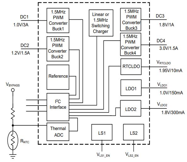
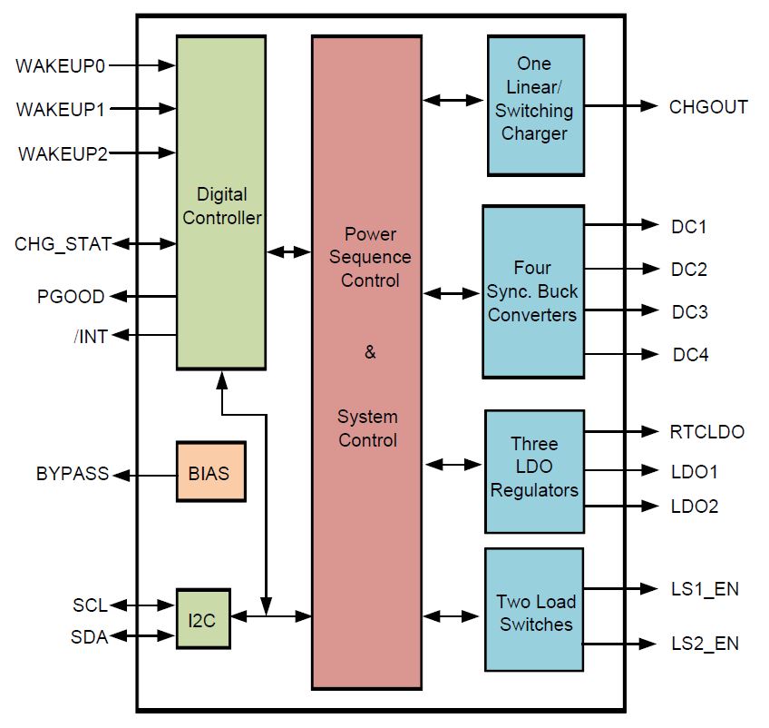
APW7713C
Active
1.5MHz PMIC for Battery Powered System with I2C Controller
Features
Charger
- Programmable Input Current Limit: 100mA, 500mA, 900mA, 1300mA, 1700mA, 2100mA, 2500mA
- Battery Charge Preconditioning
- Charge Termination and Recharge
- ±7% Charge Current Regulation
- ±7.5% Input Current Regulation
- Thermal Shutdown
- Input Over-Voltage Protection
- MOSFET Over-Current Protection
Voltage Rail
- DC2: 0.6V - 3.3V at 1.5A
- DC3: 0.6V - 3.3V at 1A
- DC4: 0.6V - 3.3V at 2A
- LDO1 0.6V - 3.3V, 150mA, Reference=0.6V
- LDO2 1.5V - 3.05V, 300mA, Controlled by I2C
General Description
The APW7713C is a Power Management IC (PMIC) with a battery powered system designed to provide complete Power Management solution for the camera applications. The IC operates from a single supply voltage of 2.7V to 6.0V allowing it to be used in Adapter/USB or 1 Cell battery applications. The APW7713C is designed to provide maximum number of regulators in the smallest available cost effective package. Included in the IC are: One selectable linear mode or switch mode charger; Four switching Buck converters for DC1/DC2/DC3/DC4, Three LDOs for Image Signal Process and RTC applications, and Two Load Switch Enable Signal Control for Wi-Fi, DRAM applications. For Charger part, when the input current limit or voltage limit is reached, the power path management automatically reduces the charge current to zero. As the system load continues to increase, the power path discharges the battery until the system power requirement is met. This supplement mode operation prevents overloading the input source. The devices initiate and complete a charging cycle without software control. It automatically detects the battery voltage and charges the battery in three phases: pre-conditioning, constant current and constant voltage. At the end of the charging cycle, the charger automatically terminates when the charge current is below a preset limit in the constant voltage phase. When the full battery falls below the recharge threshold, the charger will automatically start another charging cycle. The device provides various safety features for battery charging operation, including a pack negative thermistor monitoring, charging safety timer and over-voltage/over-current protections. For the other VRs, the IC is equipped with all the standard protection features such as current limit, over voltage and internal under voltage protection as well as thermal shutdown. The serial interface is an I2C communication interface which allows supply sequencing as well as controlled margining of ramp up and ramp down of all supplies to optimize battery power consumption. The I2C interface also allows for adjustability of VRs’ voltage and Forced PWM Mode in default operation and Auto PSM/PWM Mode in OFF mode state. Also, the power sequenc is defined by strobes and delay times under I2C Control. The device is available in a 40-pin, 5x5 mm2 thin QFN package for best thermal performance while optimizing the cost.
Features
Charger
- Available in Linear Mode or Switch Mode Charge
- High Efficiency 1.5A at Switch Mode Charge
- Single Input USB-compliant/Adapter Charge
- Programmable Input Current Limit: 100mA, 500mA, 900mA, 1300mA, 1700mA, 2100mA, 2500mA
- 4V-6V Input Operating Voltage Range
- 1.5MHz Switching Frequency for Low Profile Inductor
- Autonomous Battery Charging with or without Host Management
- Battery Charge Preconditioning
- Charge Termination and Recharge
- High Accuracy
- ±7% Charge Current Regulation
- ±7.5% Input Current Regulation
- Safety
- Thermal Shutdown
- Input Over-Voltage Protection
- MOSFET Over-Current Protection
Voltage Rail
- Provide 4 Buck Single Phase PWM Converters
- DC2: 0.6V - 3.3V at 1.5A
- DC3: 0.6V - 3.3V at 1A
- DC4: 0.6V - 3.3V at 2A
- Provide 3 LDO Output
- LDO1 0.6V - 3.3V, 150mA, Reference=0.6V
- LDO2 1.5V - 3.05V, 300mA, Controlled by I2C
- Provide 2 Load Switches Enable Signal
- 30µA Low Battery Leakage Current
- 1µA Low Battery Leakage Current in Shipping Mode
- Integrated ADC for System and Battery Monitor
- Always-On Push Bottom Monitor
- TQFN 5x5-40A Package
General Description
The APW7713C is a Power Management IC (PMIC) with a battery powered system designed to provide complete Power Management solution for the camera applications. The IC operates from a single supply voltage of 2.7V to 6.0V allowing it to be used in Adapter/USB or 1 Cell battery applications. The APW7713C is designed to provide maximum number of regulators in the smallest available cost effective package. Included in the IC are: One selectable linear mode or switch mode charger; Four switching Buck converters for DC1/DC2/DC3/DC4, Three LDOs for Image Signal Process and RTC applications, and Two Load Switch Enable Signal Control for Wi-Fi, DRAM applications. For Charger part, when the input current limit or voltage limit is reached, the power path management automatically reduces the charge current to zero. As the system load continues to increase, the power path discharges the battery until the system power requirement is met. This supplement mode operation prevents overloading the input source. The devices initiate and complete a charging cycle without software control. It automatically detects the battery voltage and charges the battery in three phases: pre-conditioning, constant current and constant voltage. At the end of the charging cycle, the charger automatically terminates when the charge current is below a preset limit in the constant voltage phase. When the full battery falls below the recharge threshold, the charger will automatically start another charging cycle. The device provides various safety features for battery charging operation, including a pack negative thermistor monitoring, charging safety timer and over-voltage/over-current protections. For the other VRs, the IC is equipped with all the standard protection features such as current limit, over voltage and internal under voltage protection as well as thermal shutdown. The serial interface is an I2C communication interface which allows supply sequencing as well as controlled margining of ramp up and ramp down of all supplies to optimize battery power consumption. The I2C interface also allows for adjustability of VRs’ voltage and Forced PWM Mode in default operation and Auto PSM/PWM Mode in OFF mode state. Also, the power sequenc is defined by strobes and delay times under I2C Control. The device is available in a 40-pin, 5x5 mm2 thin QFN package for best thermal performance while optimizing the cost.
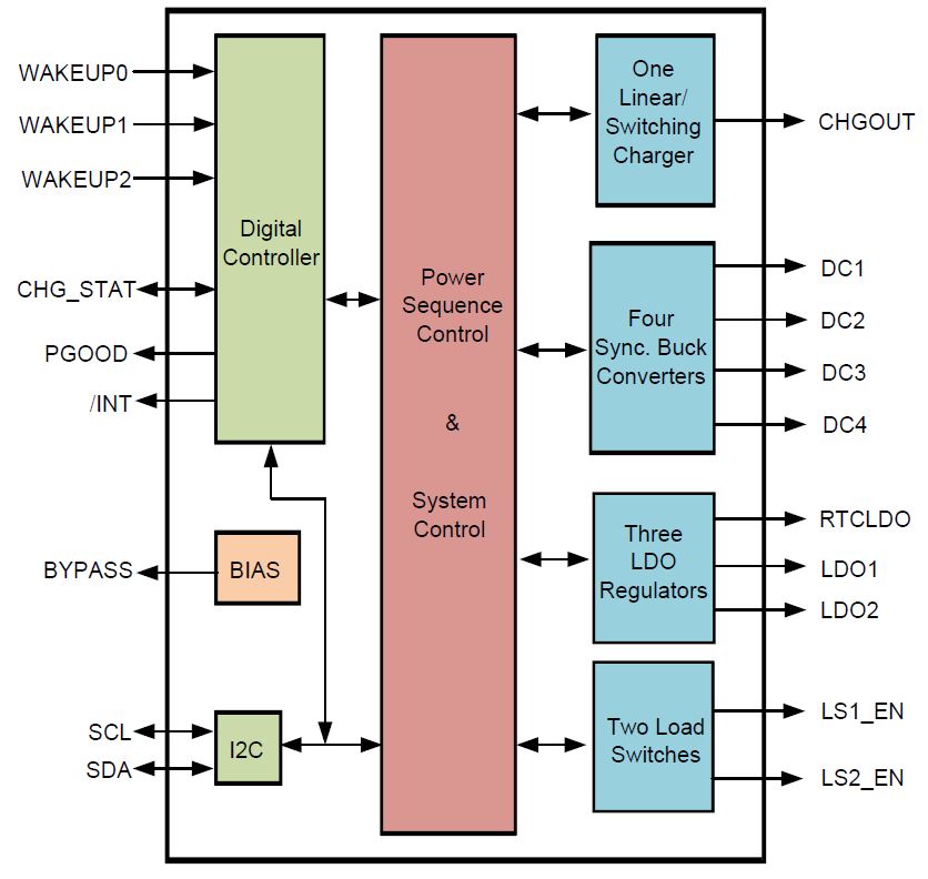
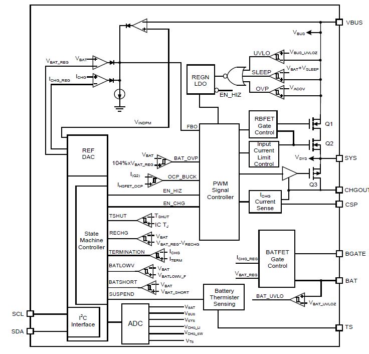
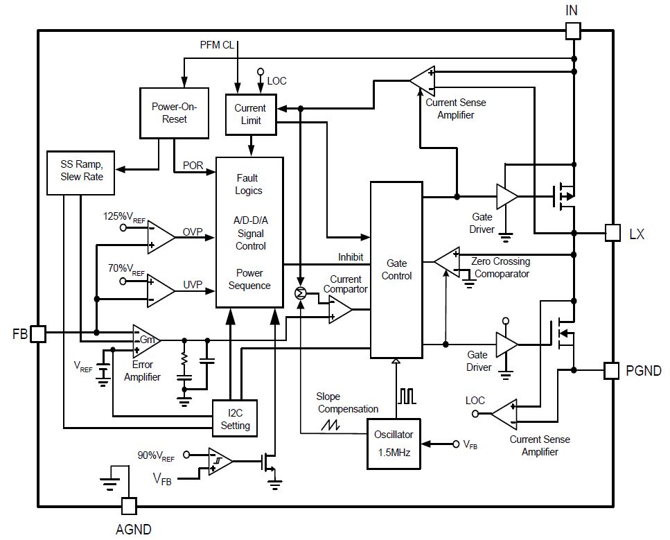

APW7713D
Active
1.5MHz PMIC for Battery Powered System with I2C Controller
Features
Charger
- Programmable Input Current Limit: 100mA, 500mA, 900mA, 1300mA, 1700mA, 2100mA, 2500mA
- Battery Charge Preconditioning
- Charge Termination and Recharge
- ±7% Charge Current Regulation
- ±7.5% Input Current Regulation
- Thermal Shutdown
- Input Over-Voltage Protection
- MOSFET Over-Current Protection
Voltage Rail
- DC2: 0.6V - 3.3V at 1.5A
- DC3: 0.6V - 3.3V at 1A
- DC4: 0.6V - 3.3V at 2A
- LDO1 0.6V - 3.3V, 150mA, Reference=0.6V
- LDO2 1.5V - 3.05V, 300mA, Controlled by I2C
General Description
The APW7713D is a Power Management IC (PMIC) with a battery powered system designed to provide complete Power Management solution for the camera applications. The IC operates from a single supply voltage of 2.7V to 6.0V allowing it to be used in Adapter/USB or 1 Cell battery applications. The APW7713D is designed to provide maximum number of regulators in the smallest available cost effective package. Included in the IC are: One selectable linear mode or switch mode charger; Four switching Buck converters for DC1/DC2/DC3/DC4, three LDOs for Image Signal Process and RTC applications. For Charger part, when the input current limit or voltage limit is reached, the power path management automatically reduces the charge current to zero. As the system load continues to increase, the power path discharges the battery until the system power requirement is met. This supplement mode operation prevents overloading the input source. The devices initiate and complete a charging cycle without software control. It automatically detects the battery voltage and charges the battery in three phases: pre-conditioning, constant current and constant voltage. At the end of the charging cycle, the charger automatically terminates when the charge current is below a preset limit in the constant voltage phase. When the full battery falls below the recharge threshold, the charger will automatically start another charging cycle. The device provides various safety features for battery charging operation, including a pack negative thermistor monitoring, charging safety timer and over-voltage/over-current protections. For the other VRs, the IC is equipped with all the standard protection features such as current limit, over voltage and internal under voltage protection as well as thermal shutdown. The serial interface is an I2C communication interface which allows supply sequencing as well as controlled margining of ramp up and ramp down of all supplies to optimize battery power consumption. The I2C interface also allows for adjustability of VRs’ voltage and Forced PWM Mode in default operation and Auto PSM/PWM Mode in OFF mode state. Also, the power sequenc is defined by strobes and delay times under I2C Control. The device is available in a 40-pin, 5x5 mm2 thin QFN package for best thermal performance while optimizing the cost.
Features
Charger
- Available in Linear Mode or Switch Mode Charge
- High Efficiency 1.5A at Switch Mode Charge
- Single Input USB-compliant/Adapter Charge
- Programmable Input Current Limit: 100mA, 500mA, 900mA, 1300mA, 1700mA, 2100mA, 2500mA
- 4V-6V Input Operating Voltage Range
- 1.5MHz Switching Frequency for Low Profile Inductor
- Autonomous Battery Charging with or without Host Management
- Battery Charge Preconditioning
- Charge Termination and Recharge
- High Accuracy
- ±7% Charge Current Regulation
- ±7.5% Input Current Regulation
- Safety
- Thermal Shutdown
- Input Over-Voltage Protection
- MOSFET Over-Current Protection
Voltage Rail
- Provide 4 Buck Single Phase PWM Converters
- DC2: 0.6V - 3.3V at 1.5A
- DC3: 0.6V - 3.3V at 1A
- DC4: 0.6V - 3.3V at 2A
- Provide 3 LDO Output
- LDO1 0.6V - 3.3V, 150mA, Reference=0.6V
- LDO2 1.5V - 3.05V, 300mA, Controlled by I2C
- Provide 2 Load Switches Enable Signal
- 30µA Low Battery Leakage Current
- 1µA Low Battery Leakage Current in Shipping Mode
- Integrated ADC for System and Battery Monitor
- Always-On Push Bottom Monitor
- TQFN5x5-40A Package
General Description
The APW7713D is a Power Management IC (PMIC) with a battery powered system designed to provide complete Power Management solution for the camera applications. The IC operates from a single supply voltage of 2.7V to 6.0V allowing it to be used in Adapter/USB or 1 Cell battery applications. The APW7713D is designed to provide maximum number of regulators in the smallest available cost effective package. Included in the IC are: One selectable linear mode or switch mode charger; Four switching Buck converters for DC1/DC2/DC3/DC4, three LDOs for Image Signal Process and RTC applications. For Charger part, when the input current limit or voltage limit is reached, the power path management automatically reduces the charge current to zero. As the system load continues to increase, the power path discharges the battery until the system power requirement is met. This supplement mode operation prevents overloading the input source. The devices initiate and complete a charging cycle without software control. It automatically detects the battery voltage and charges the battery in three phases: pre-conditioning, constant current and constant voltage. At the end of the charging cycle, the charger automatically terminates when the charge current is below a preset limit in the constant voltage phase. When the full battery falls below the recharge threshold, the charger will automatically start another charging cycle. The device provides various safety features for battery charging operation, including a pack negative thermistor monitoring, charging safety timer and over-voltage/over-current protections. For the other VRs, the IC is equipped with all the standard protection features such as current limit, over voltage and internal under voltage protection as well as thermal shutdown. The serial interface is an I2C communication interface which allows supply sequencing as well as controlled margining of ramp up and ramp down of all supplies to optimize battery power consumption. The I2C interface also allows for adjustability of VRs’ voltage and Forced PWM Mode in default operation and Auto PSM/PWM Mode in OFF mode state. Also, the power sequenc is defined by strobes and delay times under I2C Control. The device is available in a 40-pin, 5x5 mm2 thin QFN package for best thermal performance while optimizing the cost.
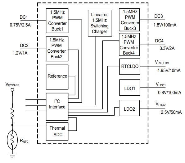
APW8856
Active
Wide Input 5.4V to 21V Power Management IC (PMIC) for High Performance Computing Applications
Key Features
Voltage Rail
- V6 (V3V3_DSW) 3.3V, 6A continuous
- V10 (VDDQ) 1.1V/1.15V/1.2V/1.35V, 7.4A continuous
- V11 (V105A) 1.05V, 10.5A continuous
- V13 (VTT) in tracking of 0.5*VDDQ voltage, 0.6A continuous
- V14 (VCC_RTC) 3V, 400mA
- V17 (VLDO_OUT) 2.8V/1.05V, 0.3A/90mA
- V5VA_LDO 5V, 100mA
- V3V3_LDO 3.3V, 100mA
- V15 (VDISO) 3.3V/1.8V switchover, 0.4A continuous
- V16 (VCCSTU) 1.05V, 190mA continuous
Power Management Controller
TQFN5x5-40 Package
General Description
The APW8856 is a Power Management IC (PMIC) designed to provide complete Power Management solution for the Rest of the Platform Power (ROP) supplies for Intel Canon Lake(*) applications. The IC operates from a single supply voltage of 5.4V to 21V allowing it to be used in 2 Cell to 4 Cell battery applications. The APW8856 is designed to provide maximum number of regulators in the smallest available cost effective package. Included in the IC are; Four Switching Buck controllers for 5V and 3.3V system voltages as well as VDDQ and 1.05V, Six LDOs for variety of applications such as memory VTT and Vpp, One internal high frequency 3A Buck regulator typically used for 1.8V supply and One Dual Input Single output switch. The PWM controllers use the ANPEC cost effective external Power Blocks APW870x family for minimum pin interface with the PMIC, while providing output currents of up to 25A capability. The IC is equipped with all the standard protection features such as over current, over voltage and internal under voltage lock out protection as well as thermal SD. The serial interface is an I2C communication interface which allows supply sequencing as well as controlled margining of ramp up and ramp down of all supplies to optimize battery power consumption. The I2C interface also allows for adjustability of Soft Start, Forced PWM/Auto PFM/PWM, power sequencing as well output discharge and IRQ. The IC is offered in a small TQFN, 5x5-40L package for best thermal performance while optimizing the cost.
(*)Intel Trade mark.
Key Features
Voltage Rail
- Provide 4 Buck Single Phase PWM Controllers
- V6 (V3V3_DSW) 3.3V, 6A continuous
- V10 (VDDQ) 1.1V/1.15V/1.2V/1.35V, 7.4A continuous
- V11 (V105A) 1.05V, 10.5A continuous
- Provide 1 Buck Single Phase PWM Converter
- Provide 6 LDO Outputs
- V13 (VTT) in tracking of 0.5*VDDQ voltage, 0.6A continuous
- V14 (VCC_RTC) 3V, 400mA
- V17 (VLDO_OUT) 2.8V/1.05V, 0.3A/90mA
- V5VA_LDO 5V, 100mA
- V3V3_LDO 3.3V, 100mA
- Provide 4 Load Switches
- V15 (VDISO) 3.3V/1.8V switchover, 0.4A continuous
- V16 (VCCSTU) 1.05V, 190mA continuous
Power Management Controller
- Support G3, S5/S4, S3, S0, DS5, DS4, DS3, nonDS3 and Connected Standby state
- POK Signal for VR power state: VDDQ_POK, RSM_ RST#_POK and V3V3_DSW_POK
- Support Several Memory Types: DDR3L, DDR4, LPDDR3, LPDDR4, DDR4RS, DDR4E, 3DXPoint
- I2C Interface for SoC Access
- Support Bit Rate 0.4MBit/s and 1MBit/s
TQFN5x5-40 Package
General Description
The APW8856 is a Power Management IC (PMIC) designed to provide complete Power Management solution for the Rest of the Platform Power (ROP) supplies for Intel Canon Lake(*) applications. The IC operates from a single supply voltage of 5.4V to 21V allowing it to be used in 2 Cell to 4 Cell battery applications. The APW8856 is designed to provide maximum number of regulators in the smallest available cost effective package. Included in the IC are; Four Switching Buck controllers for 5V and 3.3V system voltages as well as VDDQ and 1.05V, Six LDOs for variety of applications such as memory VTT and Vpp, One internal high frequency 3A Buck regulator typically used for 1.8V supply and One Dual Input Single output switch. The PWM controllers use the ANPEC cost effective external Power Blocks APW870x family for minimum pin interface with the PMIC, while providing output currents of up to 25A capability. The IC is equipped with all the standard protection features such as over current, over voltage and internal under voltage lock out protection as well as thermal SD. The serial interface is an I2C communication interface which allows supply sequencing as well as controlled margining of ramp up and ramp down of all supplies to optimize battery power consumption. The I2C interface also allows for adjustability of Soft Start, Forced PWM/Auto PFM/PWM, power sequencing as well output discharge and IRQ. The IC is offered in a small TQFN, 5x5-40L package for best thermal performance while optimizing the cost.
(*)Intel Trade mark.
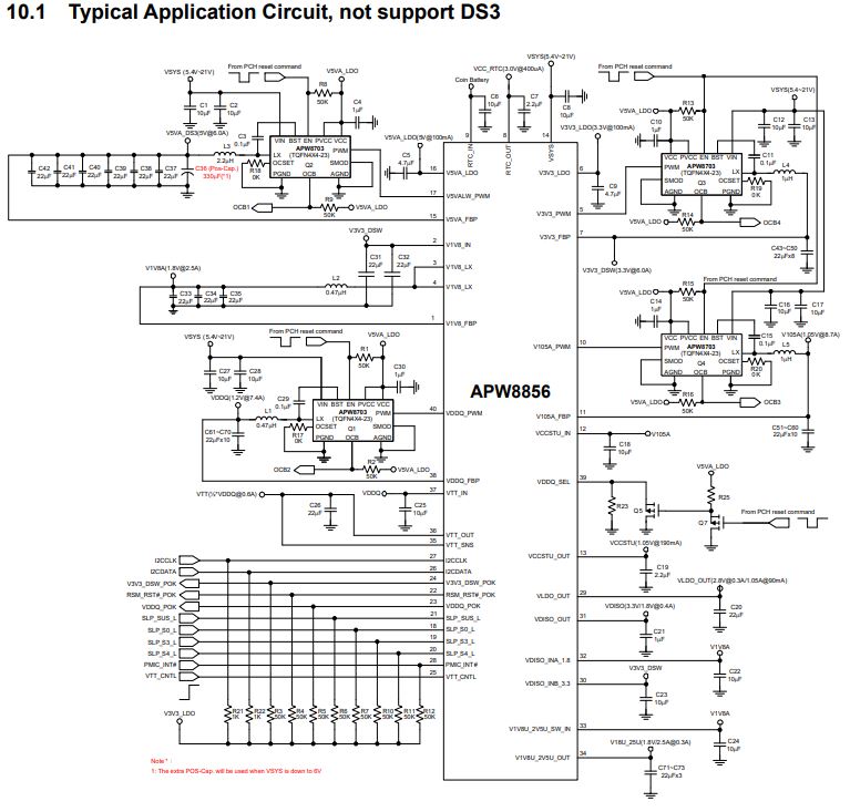
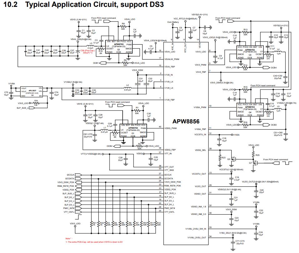
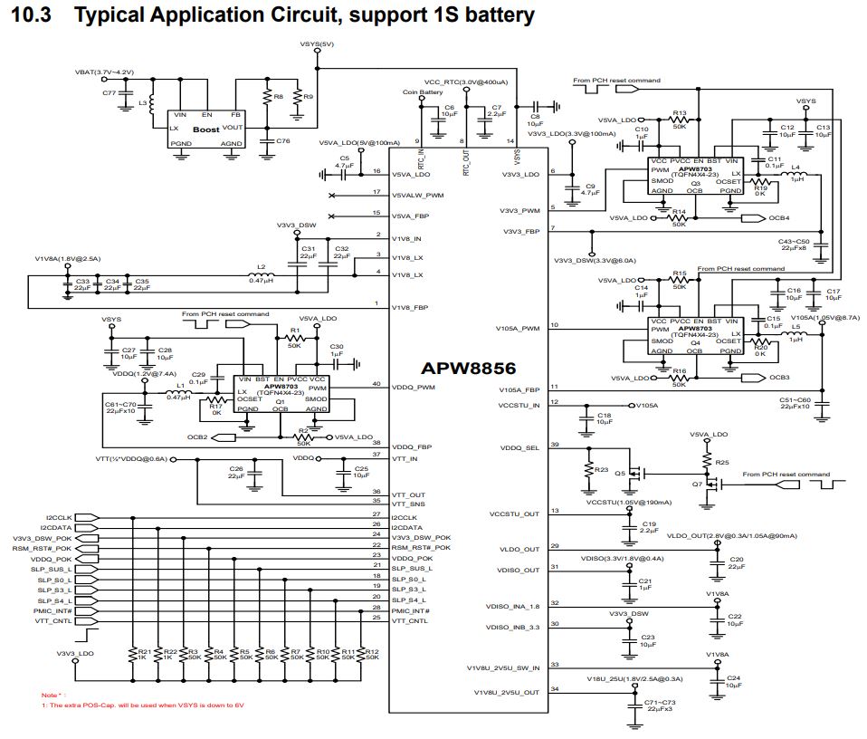
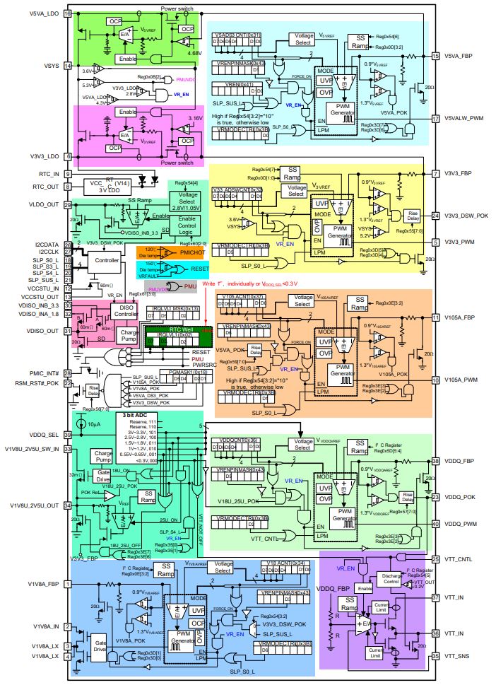
APW8857
Active
High Current, High Frequency 8 Outputs Voltage Regulator and 1 Power Switch Power
Management IC for High Performance Tablet and Ultra Notebook Applications
Key Features
Voltage Rail
- VR2 provides 5V, 8A peak output current
- VR3 provides 0.8V, 4A peak output current
- VR6 provides 0.8V, 1A peak output current
- VR7 provides a 3.3V LDO output
- VR8 provides a low quiescent LDO output for RTC
- One Power Switch with 2.5A output current
- One 5V LDO output
TQFN5x5-40 Package
General Description
The APW8857 is a Power Management IC (PMIC) designed to provide 8 Voltage regulators and 1 Power Switch for AMD’s Raven Ridge APU with ability to communicate via an I2C interface. The IC operates from a wide input voltage of 6V to 20V. There are 5 Switching Buck regulators 3 low power LDOs and 1 Power Switch that are all controlled and sequenced via the serial interface. The Buck PWM regulators consists of 3 switching controller driving external power stage such as APW8707/ APW8703/APW8706 which is capable of supplying up to 13A, 8A and 6A supply, 2 single phase switching regulators supplying up to 3A and 1A supply. The IC is equipped with all the standard protection features such as over current, over voltage and internal under voltage lock out protection. The serial interface is an I2C communication interface which allows supply sequencing as well as controlled supply ramp up and ramp down of all supplies except for the always on 1.5V LDO supplying to RTC load. The IC is offered in TQFN5x5-40 package.
Management IC for High Performance Tablet and Ultra Notebook Applications
Key Features
Voltage Rail
- Provide 3 Buck PWM Controllers with High Accuracy over Temperature
- VR2 provides 5V, 8A peak output current
- VR3 provides 0.8V, 4A peak output current
- Provide 2 Buck PWM Converters with High Accuracy over Temperature
- VR6 provides 0.8V, 1A peak output current
- Provide 3 LDO and 1 Power Switch Outputs with High Accuracy over Temperature
- VR7 provides a 3.3V LDO output
- VR8 provides a low quiescent LDO output for RTC
- One Power Switch with 2.5A output current
- One 5V LDO output
- Built in Current limit, Over Voltage protection and Over temperature protection
- I2C communication Interface for SoC Access
- Support Bit Rate 0.4MBit/s, 1MBit/s and 3.4MBit/s
- Power Sequence Control by GPIO_G3, EN_S0 and EN_S5 Pins
- Built-in Thermal Diode and I2C Reading Function for Temperature Sensing
- POK Signal for VR power state
TQFN5x5-40 Package
General Description
The APW8857 is a Power Management IC (PMIC) designed to provide 8 Voltage regulators and 1 Power Switch for AMD’s Raven Ridge APU with ability to communicate via an I2C interface. The IC operates from a wide input voltage of 6V to 20V. There are 5 Switching Buck regulators 3 low power LDOs and 1 Power Switch that are all controlled and sequenced via the serial interface. The Buck PWM regulators consists of 3 switching controller driving external power stage such as APW8707/ APW8703/APW8706 which is capable of supplying up to 13A, 8A and 6A supply, 2 single phase switching regulators supplying up to 3A and 1A supply. The IC is equipped with all the standard protection features such as over current, over voltage and internal under voltage lock out protection. The serial interface is an I2C communication interface which allows supply sequencing as well as controlled supply ramp up and ramp down of all supplies except for the always on 1.5V LDO supplying to RTC load. The IC is offered in TQFN5x5-40 package.
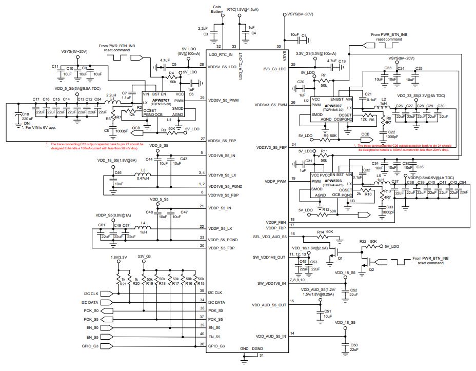
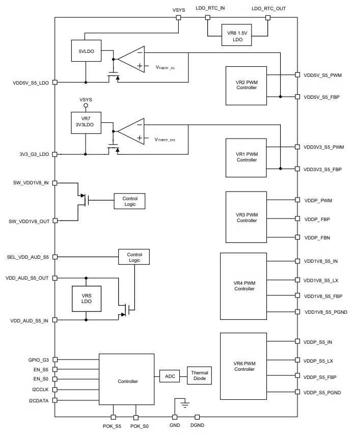
APW8858
Active
Wide Input 5.4V to 21V Power Management IC (PMIC) for High Performance Computing Applications
Features
Voltage Rail
- VR2 (VCCGI) 0.5V ~ 1.45V, 25A peak
- VR3 (VCCRAM) 1.05V ~ 1.1V, 4.5A peak
- VR6 (VDDQ) 1.1V/1.15V1.2V/1.35V, 7A peak
- VR5 (V1P2A) 1.1V ~ 1.24V, 2.5A peak
- VR8 (VPP) 2.5V, 1A continuous
Power Management Controller
TQFN5x5-40 Package
General Description
The APW8858 is a Power Management IC (PMIC) designed to provide complete Power Management solution for Intel GLK(*) plateform applications. The IC operates from a single supply voltage of 5.4V to 21V allowing it to be used in 2 Cell to 4 Cell battery applications. The APW8858 is designed to provide maximum number of regulators in the smallest available cost effective package. Included in the IC are; Four Switching Buck controllers for 5V and 3.3V system voltages as well as VDDQ and VCCRAM, Two LDOs for variety of applications such as memory VTT and VPP (V25U), Tow internal high frequency 3A Buck regulators typically used for 1.8V and 1.2V supply and One load switch (V18U). The PWM controllers use the ANPEC cost effective external Power Blocks APW870x family for minimum pin interface with the PMIC, while providing output currents of up to 25A capability. The IC is equipped with all the standard protection features such as over current, over voltage and internal under voltage lock out protection as well as thermal SD. The serial interface is an I2C communication interface which allows supply sequencing as well as controlled margining of ramp up and ramp down of all supplies to optimize battery power consumption. The I2C interface also allows for adjustability of Soft Start, Forced PWM/ Auto PFM/PWM, power sequencing as well output discharge and IRQ. The IC is offered in a small TQFN, 5x5-40L package for best thermal performance while optimizing the cost.
(*)Intel Trade mark.
Features
Voltage Rail
- Provide 4 Buck Single Phase PWM Controllers
- VR2 (VCCGI) 0.5V ~ 1.45V, 25A peak
- VR3 (VCCRAM) 1.05V ~ 1.1V, 4.5A peak
- VR6 (VDDQ) 1.1V/1.15V1.2V/1.35V, 7A peak
- Provide 2 Buck Single Phase PWM Converters
- VR5 (V1P2A) 1.1V ~ 1.24V, 2.5A peak
- Provide 2 LDO Outputs
- VR8 (VPP) 2.5V, 1A continuous
- Provide 1 Load Switche
Power Management Controller
- Support G3, S5/S4, S3, S0, DS5, DS4, DS3, and S0ix states
- POK and IRQ Signal for VR power state : PCH_PWROK, RSM_RST# and IRQ#
- Support Several Memory Types : DDR3L, DDR4, LPDDR3, LPDDR4, DDR4RS, DDR4E, 3DXPoint
- I2C Interface for SoC Access
- Support Bit Rate 0.4MBit/s and 1MBit/s
TQFN5x5-40 Package
General Description
The APW8858 is a Power Management IC (PMIC) designed to provide complete Power Management solution for Intel GLK(*) plateform applications. The IC operates from a single supply voltage of 5.4V to 21V allowing it to be used in 2 Cell to 4 Cell battery applications. The APW8858 is designed to provide maximum number of regulators in the smallest available cost effective package. Included in the IC are; Four Switching Buck controllers for 5V and 3.3V system voltages as well as VDDQ and VCCRAM, Two LDOs for variety of applications such as memory VTT and VPP (V25U), Tow internal high frequency 3A Buck regulators typically used for 1.8V and 1.2V supply and One load switch (V18U). The PWM controllers use the ANPEC cost effective external Power Blocks APW870x family for minimum pin interface with the PMIC, while providing output currents of up to 25A capability. The IC is equipped with all the standard protection features such as over current, over voltage and internal under voltage lock out protection as well as thermal SD. The serial interface is an I2C communication interface which allows supply sequencing as well as controlled margining of ramp up and ramp down of all supplies to optimize battery power consumption. The I2C interface also allows for adjustability of Soft Start, Forced PWM/ Auto PFM/PWM, power sequencing as well output discharge and IRQ. The IC is offered in a small TQFN, 5x5-40L package for best thermal performance while optimizing the cost.
(*)Intel Trade mark.