


依據歐盟施行的個人資料保護法,我們致力於保護您的個人資料並提供您對個人資料的掌握。 我們已更新並將定期更新我們的隱私權政策,以遵循該個人資料保護法。請您參照我們最新版的 隱私權聲明。
本網站使用cookies以提供更好的瀏覽體驗。如需了解更多關於本網站如何使用cookies 請按 這裏。
首頁
產品資訊
產品搜尋
SEARCH
產品類別
產品次類
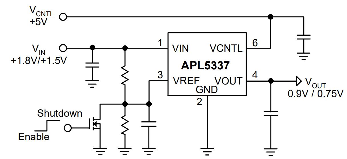
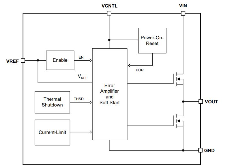
APL5337
Active
Source and Sink, 2A, Fast Transient Response Linear Regulator
Features
General Description
The APL5337 linear regulator is designed to provide a regulated voltage with bi-direction output current for DDRSDRAM termination voltage. The APL5337 integrates two power transistors to source or sink load current up to 2A. It also features internal soft-start, current-limit, thermal shutdown and enable control functions into a single chip. The internal soft-start controls the rising rate of the output voltage to prevent inrush current during start-up. The current-limit circuit detects the output current and limits the current during short-circuit or current overload conditions. The on-chip thermal shutdown provides thermal protection against any combination of overload that would create excessive junction temperatures. The output voltage of APL5337 is regulated to track the voltage on VREF pin. A proper resistor divider connected to VIN, GND, and VREF pins is used to provide a half voltage of VIN to VREF pin. In addition, connect an external ceramic capacitor and an open-drain transistor to VREF pin for external soft-start and shutdown control. Pulling and holding the voltage on VREF below the enable voltage threshold shuts down the output. The output of APL5337 will be high impedance after being shut down by VREF or the thermal shutdown function.
Features
- Provide Bi-Direction Current
- Built-in Soft-Start
- Power-On-Reset Monitoring on VCNTL Pins
- Fast Transient Response
- Stable with Ceramic Output Capacitors
- ±10mV High System Output Accuracy Over Load and Temperature Ranges
- Adjustable Output Voltage by External Resistors
- Current-Limit Protection
- On-Chip Thermal Shutdown
- Shutdown for Standby or Suspend Mode
- Simple SOP-8 and SOP-8 with Exposed Pad (SOP-8P) Packages
- Lead Free and Green Devices Available (RoHS Compliant)
General Description
The APL5337 linear regulator is designed to provide a regulated voltage with bi-direction output current for DDRSDRAM termination voltage. The APL5337 integrates two power transistors to source or sink load current up to 2A. It also features internal soft-start, current-limit, thermal shutdown and enable control functions into a single chip. The internal soft-start controls the rising rate of the output voltage to prevent inrush current during start-up. The current-limit circuit detects the output current and limits the current during short-circuit or current overload conditions. The on-chip thermal shutdown provides thermal protection against any combination of overload that would create excessive junction temperatures. The output voltage of APL5337 is regulated to track the voltage on VREF pin. A proper resistor divider connected to VIN, GND, and VREF pins is used to provide a half voltage of VIN to VREF pin. In addition, connect an external ceramic capacitor and an open-drain transistor to VREF pin for external soft-start and shutdown control. Pulling and holding the voltage on VREF below the enable voltage threshold shuts down the output. The output of APL5337 will be high impedance after being shut down by VREF or the thermal shutdown function.
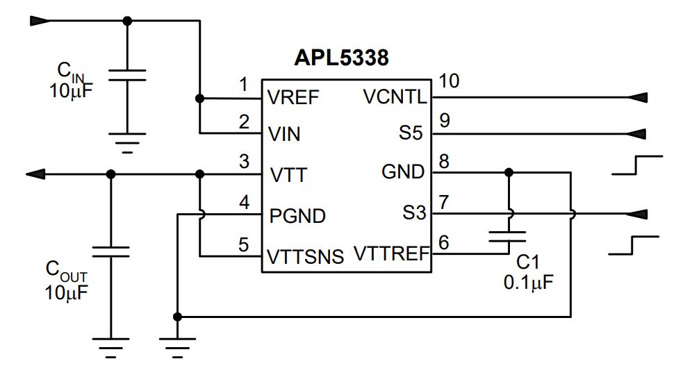
APL5338
Active
2A Bus Termination Regulator
Features
General Description
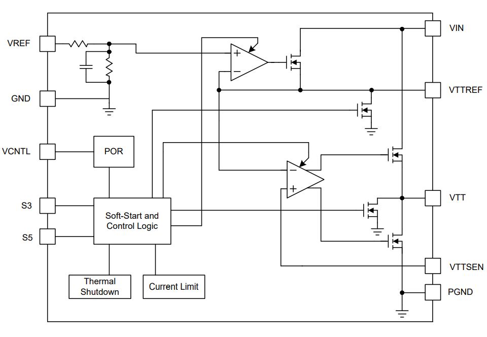
The APL5338 linear regulator is designed to provide a regulated voltage with bi-directional output current for DDR-SDRAM termination. The APL5338 integrates two power transistors to source or sink current up to 2A. It also incorporates current-limit and thermal shutdown into a single chip. The output voltage of APL5338 tracks the voltage at VREF pin. An internal resistor divider is used to provide a half voltage of VREF for VTTREF and VTT Voltage. The VTT output voltage is only requiring 10µF of ceramic output capacitance for stability and fast transient response. The S3 and S5 pins provide the sleep state for VTT (S3 state) and suspend state (S4/S5 state) for device when S5 and S3 are both pulled low the device provides the soft-off for VTT and VTTREF. The MSOP-10P and TDFN3x3-10 package with a copper pad is available which provides excellent thermal impedance.
Features
- Sourcing and Sinking Current up to 2A
- Wide Input Voltage Range: 1.2V to 3.6V
- VTT and VTTREF Voltage Tracks at Half the VREF Voltage
- VTT and VTTREF Voltage with ±10mV Accuracy
- Excellent Load Transient Response
- Stable with 10µF Ceramic Output Capacitor
- Current-Limit Protection
- Thermal Shutdown Protection
- Power-On-Reset Function on VCNTL
- S3, S5 Input Signals for ACPI States
- Small MSOP-10P and TDFN3x3-10 Packages
- Lead Free and Green Devices Available (RoHS Compliant)
General Description
The APL5338 linear regulator is designed to provide a regulated voltage with bi-directional output current for DDR-SDRAM termination. The APL5338 integrates two power transistors to source or sink current up to 2A. It also incorporates current-limit and thermal shutdown into a single chip. The output voltage of APL5338 tracks the voltage at VREF pin. An internal resistor divider is used to provide a half voltage of VREF for VTTREF and VTT Voltage. The VTT output voltage is only requiring 10µF of ceramic output capacitance for stability and fast transient response. The S3 and S5 pins provide the sleep state for VTT (S3 state) and suspend state (S4/S5 state) for device when S5 and S3 are both pulled low the device provides the soft-off for VTT and VTTREF. The MSOP-10P and TDFN3x3-10 package with a copper pad is available which provides excellent thermal impedance.
APL5338A
Active
2A Bus Termination Regulator
Features
General Description
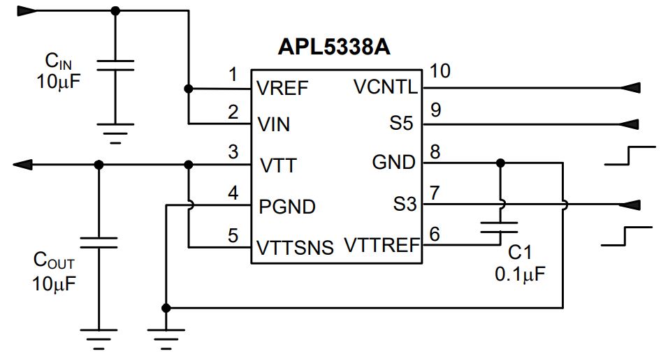
The APL5338A linear regulator is designed to provide a regulated voltage with bi-directional output current for DDR-SDRAM termination. The APL5338A integrates two power transistors to source or sink current up to 2A. It also incorporates current-limit and thermal shutdown into a single chip. The output voltage of APL5338A tracks the voltage at VREF pin. An internal resistor divider is used to provide a half voltage of VREF for VTTREF and VTT Voltage. The VTT output voltage is only requiring 10µF of ceramic output capacitance for stability and fast transient response. The S3 and S5 pins provide the sleep state for VTT (S3 state) and suspend state (S4/S5 state) for device when S5 and S3 are both pulled low the device provides the soft-off for VTT and VTTREF. The MSOP-10P and TDFN3x3-10 package with a copper pad is available which provides excellent thermal impedance.
Features
- Sourcing and Sinking Current up to 2A
- VCNTL Supply Voltage Range: 3.1V to 5.5V
- VIN Supply Voltage Range: 1.2V to 3.6V
- VTT and VTTREF Voltage Tracks at Half the VREF Voltage
- VTT and VTTREF Voltage with ±10mV Accuracy
- Excellent Load Transient Response
- Stable with 10µF Ceramic Output Capacitor
- Current-Limit Protection
- Thermal Shutdown Protection
- Power-On-Reset Function on VCNTL
- S3, S5 Input Signals for ACPI States
- Small MSOP-10P and TDFN3x3-10 Packages
- Lead Free and Green Devices Available (RoHS Compliant)
General Description
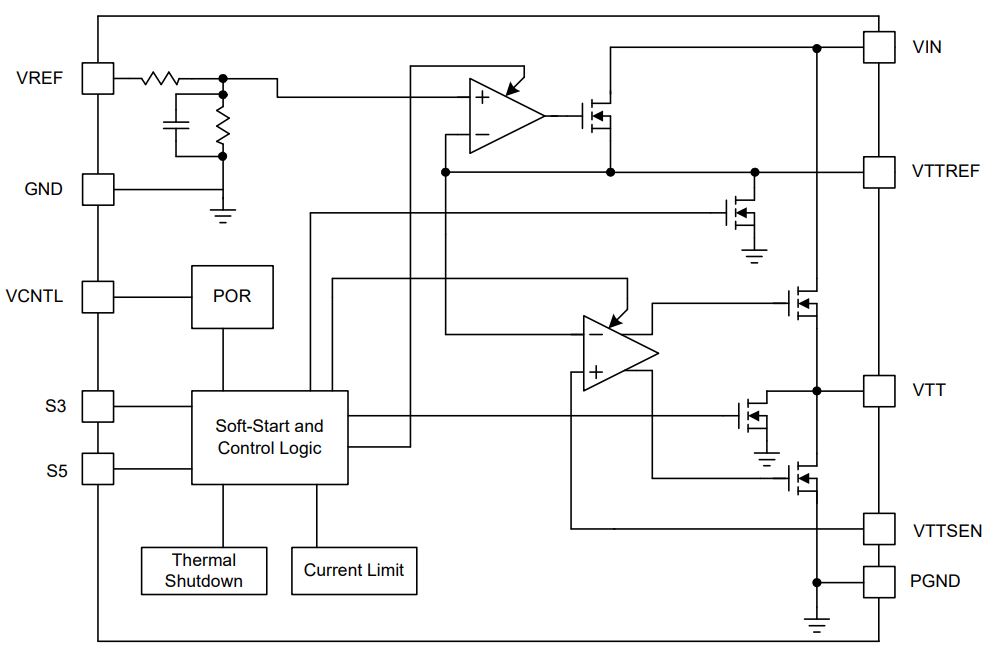
The APL5338A linear regulator is designed to provide a regulated voltage with bi-directional output current for DDR-SDRAM termination. The APL5338A integrates two power transistors to source or sink current up to 2A. It also incorporates current-limit and thermal shutdown into a single chip. The output voltage of APL5338A tracks the voltage at VREF pin. An internal resistor divider is used to provide a half voltage of VREF for VTTREF and VTT Voltage. The VTT output voltage is only requiring 10µF of ceramic output capacitance for stability and fast transient response. The S3 and S5 pins provide the sleep state for VTT (S3 state) and suspend state (S4/S5 state) for device when S5 and S3 are both pulled low the device provides the soft-off for VTT and VTTREF. The MSOP-10P and TDFN3x3-10 package with a copper pad is available which provides excellent thermal impedance.
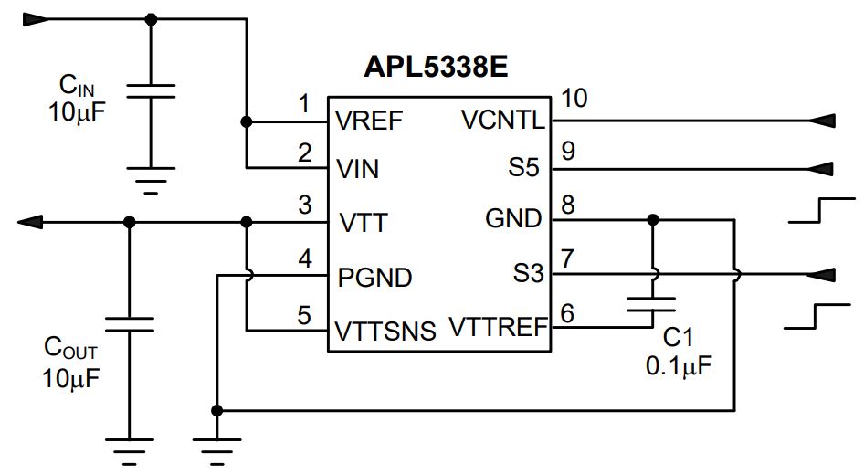
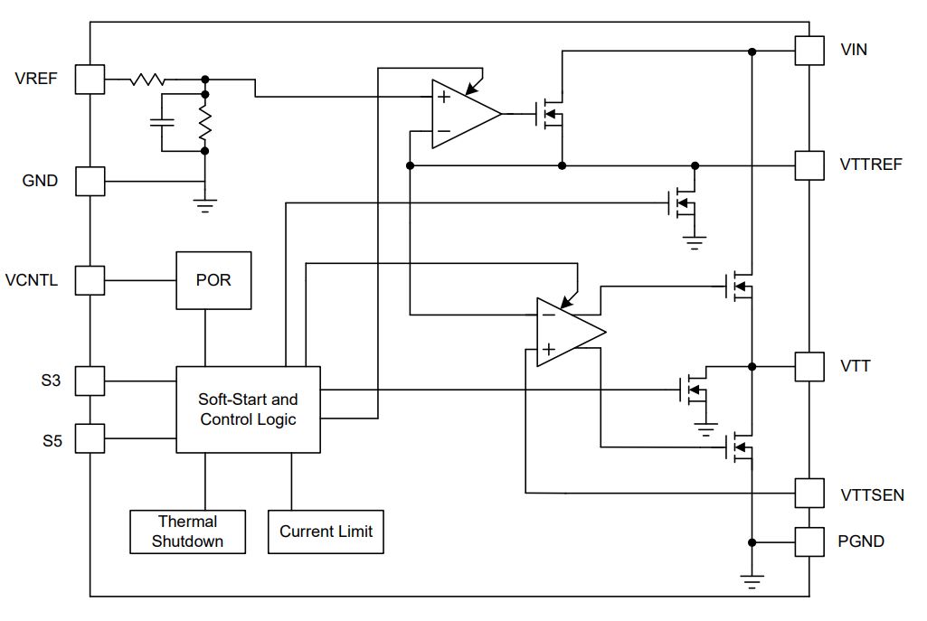
APL5338E
Active
2A Peak Sink/Source DDR Termination Regulator
Features
General Description
The APL5338E linear regulator is designed to provide a regulated voltage with bi-directional output peak current for DDR-SDRAM termination. The APL5338E integrates two power transistors to source or sink peak current up to 2A. It also incorporates current-limit and thermal shutdown into a single chip. The output voltage of APL5338E tracks the voltage at VREF pin. An internal resistor divider is used to provide a half voltage of VREF for VTTREF and VTT Voltage. The VTT output voltage is only requiring 10µF of ceramic output capacitance for stability and fast transient response. The S3 and S5 pins provide the sleep state for VTT (S3 state) and suspend state (S4/S5 state) for device when S5 and S3 are both pulled low the device provides the soft-off for VTT and VTTREF. The TDFN2x2-10 package with a copper pad is available which provides excellent thermal impedance.
Features
- Sourcing and Sinking Peak Current up to 2A
- VCNTL Supply Voltage Range: 3.1V to 5.5V
- VIN Supply Voltage Range: 1.2V to 3.6V
- VTT and VTTREF Voltage Tracks at Half the VREF Voltage
- VTT and VTTREF Voltage with ±10mV Accuracy
- Excellent Load Transient Response
- Stable with 10µF Ceramic Output Capacitor
- Current-Limit Protection
- Thermal Shutdown Protection
- Power-On-Reset Function on VCNTL
- S3, S5 Input Signals for ACPI States
- Small TDFN2x2-10 Package
- Lead Free and Green Devices Available (RoHS Compliant)
General Description
The APL5338E linear regulator is designed to provide a regulated voltage with bi-directional output peak current for DDR-SDRAM termination. The APL5338E integrates two power transistors to source or sink peak current up to 2A. It also incorporates current-limit and thermal shutdown into a single chip. The output voltage of APL5338E tracks the voltage at VREF pin. An internal resistor divider is used to provide a half voltage of VREF for VTTREF and VTT Voltage. The VTT output voltage is only requiring 10µF of ceramic output capacitance for stability and fast transient response. The S3 and S5 pins provide the sleep state for VTT (S3 state) and suspend state (S4/S5 state) for device when S5 and S3 are both pulled low the device provides the soft-off for VTT and VTTREF. The TDFN2x2-10 package with a copper pad is available which provides excellent thermal impedance.