


依據歐盟施行的個人資料保護法,我們致力於保護您的個人資料並提供您對個人資料的掌握。 我們已更新並將定期更新我們的隱私權政策,以遵循該個人資料保護法。請您參照我們最新版的 隱私權聲明。
本網站使用cookies以提供更好的瀏覽體驗。如需了解更多關於本網站如何使用cookies 請按 這裏。
Product
NEWS
Active
1MHz, High Efficiency, Step-Up Converter with Internal FET Switch
Features
- Fast Transient Response
General Description
The APW7137A is a fixed switching frequency (1 MHz typical), current-mode, step-up regulator with an integrated N-channel MOSFET. The device allows the use of small inductors and output capacitors for portable devices. The current-mode control scheme provides fast transient response and excellent output voltage accuracy. The APW7137A includes under-voltage lockout, current limit, and over-temperature shutdown to prevent damage in the event of an output overload.
Features
- Wide 2.5V to 6V Input Voltage Range
- Built-in 0.6Ω N-Channel MOSFET
- Built-in Soft-Start
- High Efficiency up to 90%
- <1µA Quiescent Current During Shutdown
- Current-Mode Operation
- Fast Transient Response
- Current-Limit Protection
- Over-Temperature Protection with Hysteresis
- Available in a Tiny 5-Pin SOT-23 and TSOT-23 Packages
General Description
The APW7137A is a fixed switching frequency (1 MHz typical), current-mode, step-up regulator with an integrated N-channel MOSFET. The device allows the use of small inductors and output capacitors for portable devices. The current-mode control scheme provides fast transient response and excellent output voltage accuracy. The APW7137A includes under-voltage lockout, current limit, and over-temperature shutdown to prevent damage in the event of an output overload.
NEWS
Active
0.6A, 5V Input, Low IQ Buck Converter
Features
General Description
The APW7581 is a synchronous buck converter adopting constant on time control mode. Due to increasing the oscillation to high frequency, the mounting area including peripheral components can be reduced. APW7581 also has low switching quiescent current to improve efficiency and battery-powered equipment using time. The APW7581 is equipped with Power-on-reset, internal soft start and over-current protection, over temperature into a single package. This device, available TDFN2x2-6 and, provides a very compact system solution external components and PCB area.
Features
- Input Voltage Range: 2.6V to 5.5V
- Low Switching Quiescent Current
- 0.6A Output Current
- Constant on Time Mode Operation
- 3MHz Switching Frequency
- Power-On-Reset Detection on VIN
- Integrated Soft Start Time
- Over-Temperature Protection
- Over-Current Protection
- Available in TDFN2x2-6 Package
General Description
The APW7581 is a synchronous buck converter adopting constant on time control mode. Due to increasing the oscillation to high frequency, the mounting area including peripheral components can be reduced. APW7581 also has low switching quiescent current to improve efficiency and battery-powered equipment using time. The APW7581 is equipped with Power-on-reset, internal soft start and over-current protection, over temperature into a single package. This device, available TDFN2x2-6 and, provides a very compact system solution external components and PCB area.
NEWS
Active
For LPDDR5/5X Memory Power Solution
Features
■ VDD2H (HV Buck): 1.065V/8A
■ VDD2L (LDO): 0.92V/1.5A
■ VDDQ (LV Buck): 0.32V/3A or 0.52V/3A By VSEL PIN Select
General Description
The APW8873 is an integrated power management IC solution for LPDDR5 and LPDDR5X memory. This device provides four power including two single buck voltage regulators VDD2H (1.065V/8A), VDDQ (0.52V or 0.32V/3A), LDO VDD2L (0.92V/1.5A) and load switch VDD1 (1.8V/1A). The APW8873 supports dynamically adjust the VDDQ output voltage by VSEL pin, thus satisfying the requirements of LPDDR5/5X DVFSC and DVFSQ applications. The APW8873 provides excellent transient response and accurate DC voltage output in either PFM or PWM Mode. In Pulse Frequency Mode (PFM), the APW8873 provides very high efficiency over light to heavy loads with loading-modulated switching frequencies. It supports multiple operational modes, S0, S3, and S4/5 by the EN and EN_VDDQ control. The APW8873 provides full protection functions, including current limit, OVP, UVP, input UVLO, and OTP. All functions are integrated in a TQFN3x3-19 package.
Features
- Wide Operating Range from 4.5V to 24V Input Voltages for HV Buck Converter
- For Output Regulations:
■ VDD2H (HV Buck): 1.065V/8A
■ VDD2L (LDO): 0.92V/1.5A
■ VDDQ (LV Buck): 0.32V/3A or 0.52V/3A By VSEL PIN Select
- Power-On-Reset Monitoring On VCC at 4.3V
- Power-On-Reset Monitoring On All Rail Input Voltage
- Support DVFSC and DVFSQ for LPDDR5/5X
- Support Power Sequence Control for LPDDR5/5X
- Built In Auto-PFM / Shutdown Control Schemes by EN Pin
- Power Good Indicator by PG Pin
- Built In Over-Temperature Protection 150oC, Hysteresis 20oC
- TQFN3x3-19p
- Built In Internal Soft-Start and Output Discharge
- UVP Setting at 60% of VOUT
- Built In Current Limit
- Built In Individual Power On/Off Control by EN Pin
- Built In Internal Soft-Start and Output Discharge
- Built In Integrated Bootstrap Forward P-CH MOSFET
- Built In Integrated MOSFET H/S RDS(ON) 28mΩ & L/S RDS(ON) 14mΩ
- UVP Setting at 60% of VOUT & OVP Setting at 125%
- Built In Current Limit Protection Using Low-Side MOS
- Built In Internal Soft-Start and Output Discharge
- UVP Setting at 60% of VOUT & OVP Setting at 125%
- Built In Current Limit
- Built In Individual Power On/Off Control by EN_ VDDQ Pin
- Built In Internal Soft-Start and Output Discharge
- Built In Integrated MOSFET H/S RDS(ON) 100mΩ & L/ S RDS(ON) 50mΩ
- UVP Setting at 60% of VOUT & OVP Setting at 125%
- Built In Current Limit Protection Using Low-Side MOS
General Description
The APW8873 is an integrated power management IC solution for LPDDR5 and LPDDR5X memory. This device provides four power including two single buck voltage regulators VDD2H (1.065V/8A), VDDQ (0.52V or 0.32V/3A), LDO VDD2L (0.92V/1.5A) and load switch VDD1 (1.8V/1A). The APW8873 supports dynamically adjust the VDDQ output voltage by VSEL pin, thus satisfying the requirements of LPDDR5/5X DVFSC and DVFSQ applications. The APW8873 provides excellent transient response and accurate DC voltage output in either PFM or PWM Mode. In Pulse Frequency Mode (PFM), the APW8873 provides very high efficiency over light to heavy loads with loading-modulated switching frequencies. It supports multiple operational modes, S0, S3, and S4/5 by the EN and EN_VDDQ control. The APW8873 provides full protection functions, including current limit, OVP, UVP, input UVLO, and OTP. All functions are integrated in a TQFN3x3-19 package.
NEWS
Active
For LPDDR5/5X Memory Power Solution
Features
■ VDD2H (HV Buck): 1.065V/8A
■ VDDQ (LV Buck): 0.32V/3A or 0.52V/3A By VSEL PIN Select
General Description
The APW8873A is an integrated power management IC solution for LPDDR5 and LPDDR5X memory. This device provides three power including two single buck voltage regulators VDD2H (1.065V/8A), VDDQ (0.52V or 0.32V/3A) and load switch VDD1 (1.8V/1A). The APW8873A supports dynamically adjust the VDDQ output voltage by VSEL pin, thus satisfying the requirements of LPDDR5/5X DVFSC and DVFSQ applications. The APW8873A provides excellent transient response and accurate DC voltage output in either PFM or PWM Mode. In Pulse Frequency Mode (PFM), the APW8873A provides very high efficiency over light to heavy loads with loading-modulated switching frequencies. It supports multiple operational modes, S0, S3, and S4/5 by the EN and EN_VDDQ control. The APW8873A provides full protection functions, including current limit, OVP, UVP, input UVLO, and OTP. All functions are integrated in a TQFN-19 3x3 package.
Features
- Wide Operating Range from 4.5V to 24V Input Voltages for HV Buck Converter
- For Output Regulations:
■ VDD2H (HV Buck): 1.065V/8A
■ VDDQ (LV Buck): 0.32V/3A or 0.52V/3A By VSEL PIN Select
- Power-On-Reset Monitoring On VCC at 4.3V
- Power-On-Reset Monitoring On All Rail Input Voltage
- Support DVFSC and DVFSQ for LPDDR5/5X
- Support Power Sequence Control for LPDDR5/5X
- Built In Auto-PFM / Shutdown Control Schemes by EN Pin
- Power Good Indicator by PG Pin
- Built In Over-Temperature Protection 150oC
- TQFN3x3-19p
- Built In Internal Soft-Start and Output Discharge
- UVP Setting at 60% of VOUT
- Built In Current Limit
- Built In Individual Power On/Off Control by EN Pin
- Built In Internal Soft-Start and Output Discharge
- Built In Integrated Bootstrap Forward P-CH MOSFET
- Built In Integrated MOSFET H/S RDS(ON) 28mΩ & L/S RDS(ON) 14mΩ
- UVP Setting at 60% of VOUT & OVP Setting at 125%
- Built In Current Limit Protection Using Low-Side MOS
- Built In Individual Power On/Off Control by EN_ VDDQ Pin
- Built In Internal Soft-Start and Output Discharge
- Built In Integrated MOSFET H/S RDS(ON) 100mΩ & L/ S RDS(ON) 50mΩ
- UVP Setting at 60% of VOUT & OVP Setting at 125%
- Built In Current Limit Protection Using Low-Side MOS
General Description
The APW8873A is an integrated power management IC solution for LPDDR5 and LPDDR5X memory. This device provides three power including two single buck voltage regulators VDD2H (1.065V/8A), VDDQ (0.52V or 0.32V/3A) and load switch VDD1 (1.8V/1A). The APW8873A supports dynamically adjust the VDDQ output voltage by VSEL pin, thus satisfying the requirements of LPDDR5/5X DVFSC and DVFSQ applications. The APW8873A provides excellent transient response and accurate DC voltage output in either PFM or PWM Mode. In Pulse Frequency Mode (PFM), the APW8873A provides very high efficiency over light to heavy loads with loading-modulated switching frequencies. It supports multiple operational modes, S0, S3, and S4/5 by the EN and EN_VDDQ control. The APW8873A provides full protection functions, including current limit, OVP, UVP, input UVLO, and OTP. All functions are integrated in a TQFN-19 3x3 package.
HOT
Active
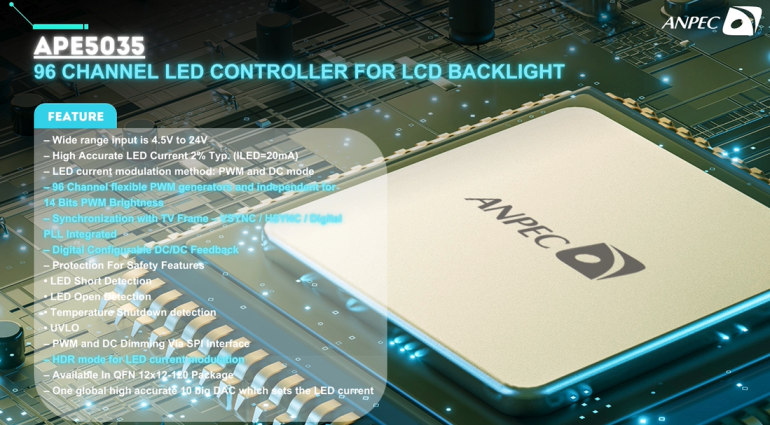
96 Channel LED Controller for LCD Backlight
Features
- LED Open Detection
- Temperature Shutdown Detection
- UVLO
General Description
The APE5035 are integrates Mosfet and 96 channel LED controller for LCD backlight. It’s high accurate LED current 2% (20mA LED current) and wide input voltage range. The APE5035 has 96 Channel flexible PWM generators and independent 14 bits PWM brightness were control LED current for every channel. In addition; It's has one global high accurate 10 bit DAC which sets the LED current. It’s synchronization with TV Frame including VSYNC/HSYNC and Digital PLL method. The APE5035 own LED current modulation method including PWM mode and DC mode. When applications have flicker frequency issue and then can using the DC mode method eliminate flicker frequency problem. The APE5035 has two pins can be digital configurable DC/DC feedback, that’s for control DC/DC architecture. As the same time; the device using programmable via SPI interface. The APE5035 owns HDR mode for modulation LED current. It’s build-in protection for safety; include LED short, LED Open, temperature shutdown protection and UVLO. The APE5035 is available in QFN12x12-120 packages.
Features
- Wide Range Input is 4.5V to 24V
- High Accurate LED Current 2% Typ. (ILED=20mA)
- LED Current Modulation Method: PWM and DC Mode
- 96 Channel Flexible PWM Generators and Independent for 14 Bits PWM Brightness
- Synchronization with TV Frame – VSYNC / HSYNC / Digital PLL Integrated
- Digital Configurable DC/DC Feedback
- Protection For Safety Features
- LED Open Detection
- Temperature Shutdown Detection
- UVLO
- PWM and DC Dimming Via SPI Interface
- HDR Mode for LED Current Modulation
- Available In QFN12x12-120 Package
- One Global High Accurate 10 big DAC which Sets the LED Current
General Description
The APE5035 are integrates Mosfet and 96 channel LED controller for LCD backlight. It’s high accurate LED current 2% (20mA LED current) and wide input voltage range. The APE5035 has 96 Channel flexible PWM generators and independent 14 bits PWM brightness were control LED current for every channel. In addition; It's has one global high accurate 10 bit DAC which sets the LED current. It’s synchronization with TV Frame including VSYNC/HSYNC and Digital PLL method. The APE5035 own LED current modulation method including PWM mode and DC mode. When applications have flicker frequency issue and then can using the DC mode method eliminate flicker frequency problem. The APE5035 has two pins can be digital configurable DC/DC feedback, that’s for control DC/DC architecture. As the same time; the device using programmable via SPI interface. The APE5035 owns HDR mode for modulation LED current. It’s build-in protection for safety; include LED short, LED Open, temperature shutdown protection and UVLO. The APE5035 is available in QFN12x12-120 packages.
HOT
Active
3-CH Buck Converter, 3-18V Input Voltage, Tiny Package
Features
- Channel 2 from 3V to 18V
- N-CH MOSFET (90mΩ) for CH2/3 High Side
- N-CH MOSFET (45mΩ) for CH1 Low Side
- N-CH MOSFET (50mΩ) for CH2/3 Low Side
General Description
The APW9304H is a three-channel synchronous mode PWM converter with 3A continuous current capability for one channel and 2.5A continuous current capability for the other channel and 1.5A continuous current capability for the other one channel. Although the switching frequency of the APW9304H is fixed at 2.1MHz, it can also change the switching frequency via the EN/SYNC pin. The APW9304H also provides a 120-degree phase shifting technique and Spread Spectrum option to minimize the noise for reducing EMI. The output voltage of each channel can be adjusted using an external resistor divider. Other features include VIN OVP, VOUT OVP, UVP, Current Limit and OTP. The internal switching frequency is set at 2.1MHz. Other features of the part include VIN OVP, OVP, UVP, Current Limit and OTP. The APW9304H is available in a TQFN 4x4-20D wettable flanks package with small size and excellent thermal capacity.
Features
- Wide Input Voltage Range:
- Channel 2 from 3V to 18V
- 3A/2.5A/1.5A Output Current on Channel 1/2/3
- Typical 0.6V ±1% Internal Reference Voltage
- Sync Pin Allows Synchronization to an External Clock from 1.8MHz to 2.4MHz
- Optimized Upper and Lower MOSFETs RDS_on for Max Efficiency:
- N-CH MOSFET (90mΩ) for CH2/3 High Side
- N-CH MOSFET (45mΩ) for CH1 Low Side
- N-CH MOSFET (50mΩ) for CH2/3 Low Side
- Built in OVP, UVP, Current Limit, VIN OVP and OTP
- Low Cost TQFN 4x4-20D Wettable Flanks Package
- High Performance or Low Cost Configuration, Auto Mode or FPWM can be Set by Mode Pin
- Spread Spectrum Option and Power On Sequence can be Configured by SEQ/SSP PIN
General Description
The APW9304H is a three-channel synchronous mode PWM converter with 3A continuous current capability for one channel and 2.5A continuous current capability for the other channel and 1.5A continuous current capability for the other one channel. Although the switching frequency of the APW9304H is fixed at 2.1MHz, it can also change the switching frequency via the EN/SYNC pin. The APW9304H also provides a 120-degree phase shifting technique and Spread Spectrum option to minimize the noise for reducing EMI. The output voltage of each channel can be adjusted using an external resistor divider. Other features include VIN OVP, VOUT OVP, UVP, Current Limit and OTP. The internal switching frequency is set at 2.1MHz. Other features of the part include VIN OVP, OVP, UVP, Current Limit and OTP. The APW9304H is available in a TQFN 4x4-20D wettable flanks package with small size and excellent thermal capacity.
NEWS
Active
2 Buck Converter+ 1 LDO PMIC for SD Express
Features
General Description
The APW7715 device is a power management solution for SD Express that integrates two high-efficiency, stepdown, DC/DC converters, one low-dropout regulator, and a flexible logic interface optimized for small solution size and high efficiency. Each DC/DC regulator switches at 2.2MHz, requiring only three small components for operation. The LDO only require small ceramic capacitors. It is highly flexible and can be reconfigured via I2C for multiple applications without the need for PCB changes. The low external component count and high configurability significantly speed time to market. Examples of configurable options include output voltage, sleep modes, input power selection for Buck2 etc.
Features
- Input Operating Range: 2.5V ~ 3.63V
- Provide Input Voltage Source Seamlessly Switched
- Built-In 2-ch Synchronous Buck Converters, 1-ch LDO
- Customized Power-On Sequence for PS5017 Controller
- Device Sleep Mode Control Pin
- Built-In Discharge Behavior
- Over-Temperature Protection
- 2.2MHz Switching Frequency for Smaller Inductor Size and Output Capacitor Size
- I2C Interface
General Description
The APW7715 device is a power management solution for SD Express that integrates two high-efficiency, stepdown, DC/DC converters, one low-dropout regulator, and a flexible logic interface optimized for small solution size and high efficiency. Each DC/DC regulator switches at 2.2MHz, requiring only three small components for operation. The LDO only require small ceramic capacitors. It is highly flexible and can be reconfigured via I2C for multiple applications without the need for PCB changes. The low external component count and high configurability significantly speed time to market. Examples of configurable options include output voltage, sleep modes, input power selection for Buck2 etc.
HOT
Active
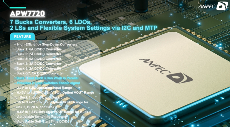
The PMIC Features 7 Buck Converters, 6 LDOs, 2 LSs, and Flexible System Settings Via I2C and MTP
Features
Charger
- BUCK2: 1V ~ 3.4V, 10mV Step, 2A
- BUCK3: 0.45V ~ 1.275V, 3.75mV Step, 6A
- BUCK4: 0.6V ~ 1.54V, 5mV Step, 3A
- BUCK5: 0.45V ~ 1.275V, 3.75mV Step, 3A
- BUCK6: 1V ~ 3.4V, 10mV Step, 2A
- BUCK7: 1V ~ 3.4V, 10mV Step, 2A
- LDO2: 1V ~ 3.4V, 50mV Step, 300mA
- LDO3: 1V ~ 3.4V, 50mV Step, 300mA
- LDO4: 0.6V ~ 1.23V, 10mV Step, 200mA
- LDO5: 1V ~ 3.4V, 50mV Step, 150mA
- LDO6: 0.6V ~ 1.23V, 10mV Step, 300mA
General Description
The APW7720 is a Power Management IC (PMIC) designed to provide complete power management solution for Surveillance Cam, IP Cam and Video Conference-Call applications. It integrates a PWM power stage and well-designed control circuitry to minimize the need for external components, thereby simplifying layout in constrained PCB areas. This device features 7 adjustable output voltage buck converters, 6 adjustable output voltage low-noise LDOs, and 2 sets of built-in logic control signal outputs selectable at 1.8V or 3.3V, all of which can be configured via I2C. The APW7720 features protection functions against over current, output over/under voltage, VSYS over voltage and over temperature to prevent catastrophic failure. Fault events also cause a state change on the PGOOD and /INT output pins, which is helpful for interrupt control or debugging. Additionally, it integrates two Under-Voltage Lockout (UVLO) features to monitor the voltages of VSYS and VINLDO1, thereby preventing improper operation during power-up and power-down. An I2C interface is provided in this device for the system designer to customize settings or presets using Multi-Time Programmable (MTP) features, including power-up/down sequence, output voltage, ramp-up/down time, power-good delay time, watchdog timer, PWM switching frequency, forced PWM mode or automatic PFM/PWM mode, output discharge mode or ramp-down mode, and latch off mode or auto-reboot mode. These customizable MTP settings give system designers the flexibility to optimize performance for various use cases, ensuring efficient and reliable operation. The APW7720 is halogen and lead free device, compliant with RoHS, available in TQFN6x6-52B package.
Features
Charger
- 3.5V to 5.5V Operating Input Range
- Built-in UVLO, OVP for Main Input Voltage
- Built-in 7 High-Efficiency Step-Down Converters
- BUCK2: 1V ~ 3.4V, 10mV Step, 2A
- BUCK3: 0.45V ~ 1.275V, 3.75mV Step, 6A
- BUCK4: 0.6V ~ 1.54V, 5mV Step, 3A
- BUCK5: 0.45V ~ 1.275V, 3.75mV Step, 3A
- BUCK6: 1V ~ 3.4V, 10mV Step, 2A
- BUCK7: 1V ~ 3.4V, 10mV Step, 2A
- Configurable Dual Phase or Single Phase Regulator for BUCK1/BUCK3
- Configurable PWM Switching Frequency from 400kHz to 2.5MHz
- Programmable Automatic PFM/PWM Mode, Forced PWM Mode
- Adjustable Ramp-Up Time and Ramp-Down Time for BUCK1 ~ BUCK7
- Built-in RTC Dedicated LDO and 5 Low-Noise LDOs
- LDO2: 1V ~ 3.4V, 50mV Step, 300mA
- LDO3: 1V ~ 3.4V, 50mV Step, 300mA
- LDO4: 0.6V ~ 1.23V, 10mV Step, 200mA
- LDO5: 1V ~ 3.4V, 50mV Step, 150mA
- LDO6: 0.6V ~ 1.23V, 10mV Step, 300mA
- Configurable LDO2/3 Output 1.8V/3.3V by LDO2/3_SEL Pin
- Built-in Dual Sets of Logic Control Signal Outputs, Selectable at 1.8V or 3.3V
- Built-in Double Thermal Protection with Temperature Alarm and Thermal Shutdown
- Built-in Output Over Voltage Protection (OVP), Output Under Voltage Protection (UVP), Current Limit
- Built-in Interrupt Control and Reporting by /INT Pin
- Built-in PGOOD to Indicate the Power Status of All VRs
- I2C Bus and User Programmable MTP
- Programmable Power Sequence Control for All Channels Via I2C
- Built-in Watchdog Timer, Programmable Via I2C
- Supports Self-Refresh Mode Via Off Mode Function
- Available in TQFN6x6-52B Package
General Description
The APW7720 is a Power Management IC (PMIC) designed to provide complete power management solution for Surveillance Cam, IP Cam and Video Conference-Call applications. It integrates a PWM power stage and well-designed control circuitry to minimize the need for external components, thereby simplifying layout in constrained PCB areas. This device features 7 adjustable output voltage buck converters, 6 adjustable output voltage low-noise LDOs, and 2 sets of built-in logic control signal outputs selectable at 1.8V or 3.3V, all of which can be configured via I2C. The APW7720 features protection functions against over current, output over/under voltage, VSYS over voltage and over temperature to prevent catastrophic failure. Fault events also cause a state change on the PGOOD and /INT output pins, which is helpful for interrupt control or debugging. Additionally, it integrates two Under-Voltage Lockout (UVLO) features to monitor the voltages of VSYS and VINLDO1, thereby preventing improper operation during power-up and power-down. An I2C interface is provided in this device for the system designer to customize settings or presets using Multi-Time Programmable (MTP) features, including power-up/down sequence, output voltage, ramp-up/down time, power-good delay time, watchdog timer, PWM switching frequency, forced PWM mode or automatic PFM/PWM mode, output discharge mode or ramp-down mode, and latch off mode or auto-reboot mode. These customizable MTP settings give system designers the flexibility to optimize performance for various use cases, ensuring efficient and reliable operation. The APW7720 is halogen and lead free device, compliant with RoHS, available in TQFN6x6-52B package.
Active
-1A, -12V Inverting Converter With PSM Mode
Features
- Under Voltage Protection and Hiccup Mode
- Current Limited
- Over Temperature Protection
- BST to SW POR function
General Description
APW7393 is an inverting Buck-Boost converter. Integrated 70mΩ high side and 60mΩ low side power MOSFET. Can generating a negative output voltage and provides an output current up to -1A. The APW7393 is equipped with an automatic PSM/PWM mode operation when MODE pin connecting to VOUT pin. At light load, the IC operates in the PSM mode to reduce the switching losses. At heavy load, APW7393 works in PWM mode with a fixed switching frequency of 500kHz. If MODE pin connecting to VIN pin, converter working in force PWM mode. Built-in EN function reference voltage, can simplify enable function in inverting converter application. Give a voltage more than 2V on EN to GND pin, IC VOUT will turn on with soft-start function. The APW7393 is also equipped with Power-on-reset, soft start, enable/disable and whole protections (over-voltage, hiccup mode, over-temperature and current-limit) into a single package.
Features
- Operating Input Voltage Range 9V to 14V
- Output Current Up to -1A
- Reference Voltage: 0.8V
- Efficiency Up to 90% at -1A Loading
- Current Mode with PSM for Fast Response and Higher Efficiency
- Fixed 500kHz Switching Frequency
- Protections:
- Under Voltage Protection and Hiccup Mode
- Current Limited
- Over Temperature Protection
- BST to SW POR function
- Internal Soft-Start
General Description
APW7393 is an inverting Buck-Boost converter. Integrated 70mΩ high side and 60mΩ low side power MOSFET. Can generating a negative output voltage and provides an output current up to -1A. The APW7393 is equipped with an automatic PSM/PWM mode operation when MODE pin connecting to VOUT pin. At light load, the IC operates in the PSM mode to reduce the switching losses. At heavy load, APW7393 works in PWM mode with a fixed switching frequency of 500kHz. If MODE pin connecting to VIN pin, converter working in force PWM mode. Built-in EN function reference voltage, can simplify enable function in inverting converter application. Give a voltage more than 2V on EN to GND pin, IC VOUT will turn on with soft-start function. The APW7393 is also equipped with Power-on-reset, soft start, enable/disable and whole protections (over-voltage, hiccup mode, over-temperature and current-limit) into a single package.
Active
1MHz, High Efficiency, Step-Up Converter with Internal FET Switch
Features
- Fast Transient Response
General Description
The APW7137 is a fixed switching frequency (1MHz typical), current-mode, step-up regulator with an integrated N-channel MOSFET. The device allows the usage of small inductors and output capacitors for portable devices. The current-mode control scheme provides fast transient response and good output voltage accuracy. The APW7137 includes under-voltage lockout, current limit, and over-temperature shutdown preventing damage in the event of an output overload.
Features
- Wide 2.5V to 6V Input Voltage Range
- Built-in 0.6Ω N-Channel MOSFET
- Built-in Soft-Start
- High Efficiency up to 90%
- <1µA Quiescent Current During Shutdown
- Current-Mode Operation
- Fast Transient Response
- Current-Limit Protection
- Over-Temperature Protection with Hysteresis
- Available in a Tiny 5-Pin SOT-23 and TSOT-23 Packages
- Lead Free and Green Devices Available (RoHS Compliant)
General Description
The APW7137 is a fixed switching frequency (1MHz typical), current-mode, step-up regulator with an integrated N-channel MOSFET. The device allows the usage of small inductors and output capacitors for portable devices. The current-mode control scheme provides fast transient response and good output voltage accuracy. The APW7137 includes under-voltage lockout, current limit, and over-temperature shutdown preventing damage in the event of an output overload.
Active
Dual Channel Synchronous Buck PWM Controller
Features
- Discontinuous Conduction Mode in Light Load to Increase Efficiency (VEN=2V)
- Sence External RSENSE (option 2)
General Description
The APW7391 is a dual channel voltage mode, synchronous PWM controller which drives dual N-channel MOSFETs. The device integrates monitoring and protection functions into a single package, provides two controlled power output with under-voltage and overcurrent protections. The APW7391 provides excellent regulation for output load variation. The internal 1.0V temperature compensated reference voltage provides high accuracy of 0.8% over line and load regulation. The PWM switching frequency is adjustable from 50kHz to 350kHz. The APW7391 has been equipped with excellent protection functions: POR, IMON, OCP, SCP, UVP, OVP OTP. The Power-On-Reset (POR) circuit can monitor the VCC input voltage to make sure the supply voltage is valid. The APW7391 adopts either the external power inductor’s DCR or an external accurate sense resistor to sense the output current. The output current information is reported at IMON pin whose output voltage is proportional to output current. During the PWM switching, the APW7391 has OCP and SCP protections. When the load current exceeds the OCP or SCP threshold, the APW7391 shuts off its PWM switcher to prevent catastrophic failure caused by abnormal load or short-circuit. The APW7391 senses its FB pin for output UVP and OVP protection, which is 50% and 120% of reference voltage respectively. When the UVP or OVP occurs, the APW7391 latches off the PWM switcher. APW7391 has over temperature protection. When the die temperature is above 150°C, the APW7391 ceases PWM operation and recover normal operation when the die temperature drops by 40°C. The APW7391 is available in SSOP-24 and SSOP-24P packages, which is compliant with RoHS.
Features
- Single 12V Power Supply Required
- Excellent Output Voltage Regulation
- Simple Single Loop Control Design
- Programmable Frequency Range from 50kHz ~ 350kHz
- CCM/DCM Operation Selectable by EN Pin
- Discontinuous Conduction Mode in Light Load to Increase Efficiency (VEN=2V)
- Output Current Monitor (IMON Pin)
- Integrated Soft-Start and Soft-Off
- Support Pre-Biased Power-On
- Output Power Line Compensation
- Phase Shift 180°
- Integrated Boot-Strap Diode
- Over-Current and Short-Circuit Protection
- Sence External RSENSE (option 2)
- 120% Over-Voltage Protection
- 50% Under-Voltage Protection
- Over-Temperature Protection
- Available in SSOP-24 and SSOP-24P Packages
General Description
The APW7391 is a dual channel voltage mode, synchronous PWM controller which drives dual N-channel MOSFETs. The device integrates monitoring and protection functions into a single package, provides two controlled power output with under-voltage and overcurrent protections. The APW7391 provides excellent regulation for output load variation. The internal 1.0V temperature compensated reference voltage provides high accuracy of 0.8% over line and load regulation. The PWM switching frequency is adjustable from 50kHz to 350kHz. The APW7391 has been equipped with excellent protection functions: POR, IMON, OCP, SCP, UVP, OVP OTP. The Power-On-Reset (POR) circuit can monitor the VCC input voltage to make sure the supply voltage is valid. The APW7391 adopts either the external power inductor’s DCR or an external accurate sense resistor to sense the output current. The output current information is reported at IMON pin whose output voltage is proportional to output current. During the PWM switching, the APW7391 has OCP and SCP protections. When the load current exceeds the OCP or SCP threshold, the APW7391 shuts off its PWM switcher to prevent catastrophic failure caused by abnormal load or short-circuit. The APW7391 senses its FB pin for output UVP and OVP protection, which is 50% and 120% of reference voltage respectively. When the UVP or OVP occurs, the APW7391 latches off the PWM switcher. APW7391 has over temperature protection. When the die temperature is above 150°C, the APW7391 ceases PWM operation and recover normal operation when the die temperature drops by 40°C. The APW7391 is available in SSOP-24 and SSOP-24P packages, which is compliant with RoHS.
Active
USB Power-Distribution Switches
Features
- HBM with over 2kV
- CDM with over 500V at VIN Pin
General Description
The APL3576A is designed for desktop adapter applications. The low on resistance N-channel MOSFET power switch can satisfy the voltage drop requirements of USB specification. Protection features include current-limit protection, short-circuit protection, over-temperature protection, wrong VIN input voltage protection, surge protection, and reverse current blocking. Other features include a deglitched ACOK output to indicate the fault condition and an enable input to enable or disable the device.
Features
- VIN Input Voltage Range: 4.5 to 25V
- 30V Absolute Ratings at VIN Pin
- 15A Output Current Capability
- Adjustable Soft-start Time by SS Pin
- Fast Over Current Protection Response Time
- Wrong VIN Input Voltage Protection
- Fault Report on ACOK Pin
- Built-in Surge Protection when Surge Voltage over 27V
- Built-in Thermal Shutdown Protection
- Built-in Enable / Shutdown Control by DPREN Pin
- Integrated Internal Charge Pump
- Built-in Programmable Short Circuit or Over Current Protection Threshold Setting by ALSET Pin
- ESD Protection:
- HBM with over 2kV
- CDM with over 500V at VIN Pin
- Over-Temperature Protection
- TQFN4x4-24 Package
General Description
The APL3576A is designed for desktop adapter applications. The low on resistance N-channel MOSFET power switch can satisfy the voltage drop requirements of USB specification. Protection features include current-limit protection, short-circuit protection, over-temperature protection, wrong VIN input voltage protection, surge protection, and reverse current blocking. Other features include a deglitched ACOK output to indicate the fault condition and an enable input to enable or disable the device.
Active
The PMIC with 4 Buck Converters, 3 LDOs, 2 Load Switches, and Flexible System Settings Via I2C Controller
Features
Voltage Rail
- DC2: 0.5V - 3.3V at 1.5A
- DC3: 0.6V - 3.3V at 1A
- DC4: 0.6V - 3.3V at 1.5A
- LDO1 0.6V - 3.3V, 150mA, Reference=0.6V
- LDO2 1.2V - 2.44V, 150mA, Controlled by I2C
General Description
The APW7708 is a Power Management IC (PMIC) designed to provide complete Power Management solution for the driving video recorder (DVR) applications. The APW7708 is designed to provide maximum number of regulators in the smallest available cost eff ective package. Included in the IC are: Four Synchronous Buck Converters for DC1 ~ DC4; Three LDOs with one for RTC application, and Two Load Switch Enable Signal Control for external load switches application. For the Bucks, the IC is equipped with all the standard protection features such as current limit, over voltage and internal under voltage protection as well as thermal shutdown. The serial interface is an I2C communication interface. The I2C interface also allows for adjustability of VRs’ voltage. Also, the power sequence is defi ned by strobes and delay times under I2C Control. The device is available in a 40-pin, 5x5 mm2 thin QFN package for best thermal performance while optimizing the cost.
Features
Voltage Rail
- Provide 4 Buck Single Phase PWM Converters
- DC2: 0.5V - 3.3V at 1.5A
- DC3: 0.6V - 3.3V at 1A
- DC4: 0.6V - 3.3V at 1.5A
- Provide 3 LDO Output
- LDO1 0.6V - 3.3V, 150mA, Reference=0.6V
- LDO2 1.2V - 2.44V, 150mA, Controlled by I2C
- Provide 2 Load Switches Enable Signal
- Current Limit Protection
- Output Under-Voltage Protection
- Output Over-Voltage Protection for Bucks
- Thermal Shutdown Protection
- TQFN 5x5-40A Package
General Description
The APW7708 is a Power Management IC (PMIC) designed to provide complete Power Management solution for the driving video recorder (DVR) applications. The APW7708 is designed to provide maximum number of regulators in the smallest available cost eff ective package. Included in the IC are: Four Synchronous Buck Converters for DC1 ~ DC4; Three LDOs with one for RTC application, and Two Load Switch Enable Signal Control for external load switches application. For the Bucks, the IC is equipped with all the standard protection features such as current limit, over voltage and internal under voltage protection as well as thermal shutdown. The serial interface is an I2C communication interface. The I2C interface also allows for adjustability of VRs’ voltage. Also, the power sequence is defi ned by strobes and delay times under I2C Control. The device is available in a 40-pin, 5x5 mm2 thin QFN package for best thermal performance while optimizing the cost.
Application

為消費性、可攜式/IOT和車用電子產品,提供單獨高壓DC/DC電源解決方案和高整合/客製化 PMICs
提供低元件數量設計和低靜態電流的特性,是空間受限的 PCBs 和電池供電應用的理想選擇

茂達電子為汽車電子提供了完整的電源解決方案,規劃支援輸入電壓範圍從 3V 到 42V,並提供輸出電流範圍從 1A 到 6A。
此外,茂達電子致力於降低 EMI (Out-of-Phase operation & Spread spectrum),並提供...
About Us
品質保證 是茂達對社會的承諾
茂達電子成立於1997年10月,為台灣第一家掛牌之功率IC設計公司。
為滿足高端市場需求,茂達電子於2000年啟動轉型,
大幅建置數位/混合IC設計能量與產品線,
成為以功率管理與驅動為核心之混合訊號IC供應商,
提供客戶完整的功率與混合訊號解決方案。

持續改善

客戶滿意

品質承諾

全員參與

精準到位


DATE
2026/07/15
產品訊息
The APX9351 Provides All the Circuitry for Sensor-Less Speed Control of Three-Phase Brushless DC Motor
The APX9351 Provides All the Circuitry for Sensor-Less Speed Control of Three-Phase Brushless DC Motor.
DATE
2026/07/08
公司訊息
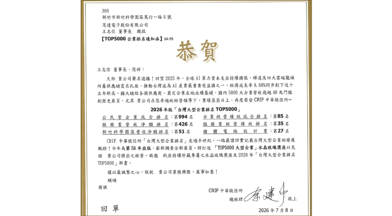
茂達電子榮獲中華徵信所評選為「台灣大型企業排名TOP5000」
茂達電子榮獲中華徵信所評選為2025年「台灣大型企業排名TOP5000」新竹科學園區營收淨額排名第51名,積體電路設計業第27名。
DATE
2026/06/25
公司訊息
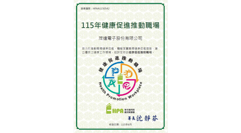
茂達電子經衛生福利部國民健康署評定符合「115年健康促進推動職場」
茂達電子致力於推動職場健康促進,積極落實職場健康促進措施,建立優良之健康工作環境,經評定符合健康促進推動職場。
DATE
2026/05/15
產品訊息
Discover the APE5035: 96 Channel LED Local Dimming Controller for LCD Backlight
The APE5035 integrates a MOSFET and a 96-channel LED controller for LCD backlighting. It provides highly accurate LED current control (2% with a 30mA LED current) and operates over a wide input voltage range.

DATE
2026/05/13
社會參與
【員工照護】健康講座:壓力大長皮蛇?連癌症都能打預防針?解鎖你的成人專屬防護罩!
工作壓力大會影響健康嗎?其實壓力可能降低免疫力,甚至引發如皮蛇等疾病;而部分疾病可透過疫苗提前預防。


DATE
2026/04/17
社會參與
【環境保護】「世界地球日」舉辦淨灘與環境教育活動
為了響應「世界地球日」,茂達電子福委會於近日圓滿舉辦了淨灘活動。本次活動共有94位同仁參與,總計清理出高達523公斤的垃圾!

DATE
2026/03/18
社會參與
【社會關懷】狗狗翻譯官: 聽懂狗狗的「聲音密碼」
ESG生命教育講座邀請「新竹動物保護協會」與同仁分享「如何聽懂狗狗的心聲」。
從「噪音」到「訊息」:一場認知的翻轉
DATE
2026/03/16
產品訊息
APW7720 PMIC Features 7 Buck Converters, 6 LDOs, 2 LSs and Flexible System Settings Via I2C and MTP
The APW7720 Power Management IC (PMIC) only requires one supply input, LI-ION Battery (3.0~4.3V) or 5.0V, generates seven PWM step-down converters, five low-noise LDOs, one RTC-dedicated LDO, and two enable logic control.

DATE
2026/01/15
產品訊息
Discover the APW8895: a Synchronous NVDC Buck-Boost Switching Charger Controller
This versatile device seamlessly transitions between buck, buck-boost, and boost modes, catering to 2- to 4-cell Li-ion batteries.


DATE
2025/11/14
產品訊息
ANPEC Collaborates with Valens Semiconductor to Deliver Optimized Automotive Power Solutions
We are thrilled to announce a collaboration between ANPEC and Valens to develop cutting-edge solutions for the automotive industry. The companies collaborated on integrating ANPEC's APW9304H, an AEC-Q100 qualified Power Management IC, known for its ultra-low EMI feature and flexible power sequencing, to Valens' VA7000 and VA6000 series product reference designs for ADAS, autonomous driving and in-car entertainment systems.
DATE
2025/11/14
產品訊息
APW9304H is an Ultra-low EMI Triple Buck Converter and Designed for Automotive Applications (AEC-Q100)
Meet the APW9304H, an advanced triple buck converter designed for automotive excellence (AEC-Q100).

DATE
2025/09/03
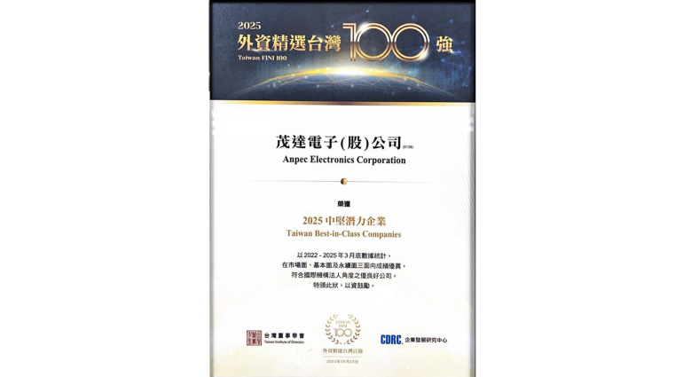
公司訊息
茂達電子榮獲「2025 外資精選台灣100強 之中堅潛力企業」
評選標準涵蓋市場面、基本面、永續面三大指標。茂達電子從2194家台灣上市櫃及興櫃企業中脫穎而出,榮獲「中堅潛力獎」。


DATE
2025/07/24
社會參與
【社會關懷】一袋熱血,一份希望!
茂達堅信,點滴善舉能匯聚成無限正能量,活動期間,全體員工共捐獻了 140袋珍貴血液,每一袋都承載著生命的希望,為亟需幫助的患者點燃了重生的曙光。


DATE
2024/12/25
公司訊息
茂達電子榮獲教育部體育署頒贈「2024年運動企業認證」
茂達電子榮獲教育部體育署頒贈「2024年運動企業認證」,未來將秉持精益求精之運動精神,持續推動職場健康及員工運動風氣。