


依據歐盟施行的個人資料保護法,我們致力於保護您的個人資料並提供您對個人資料的掌握。 我們已更新並將定期更新我們的隱私權政策,以遵循該個人資料保護法。請您參照我們最新版的 隱私權聲明。
本網站使用cookies以提供更好的瀏覽體驗。如需了解更多關於本網站如何使用cookies 請按 這裏。
首頁
產品資訊
產品搜尋
SEARCH
產品類別
產品次類
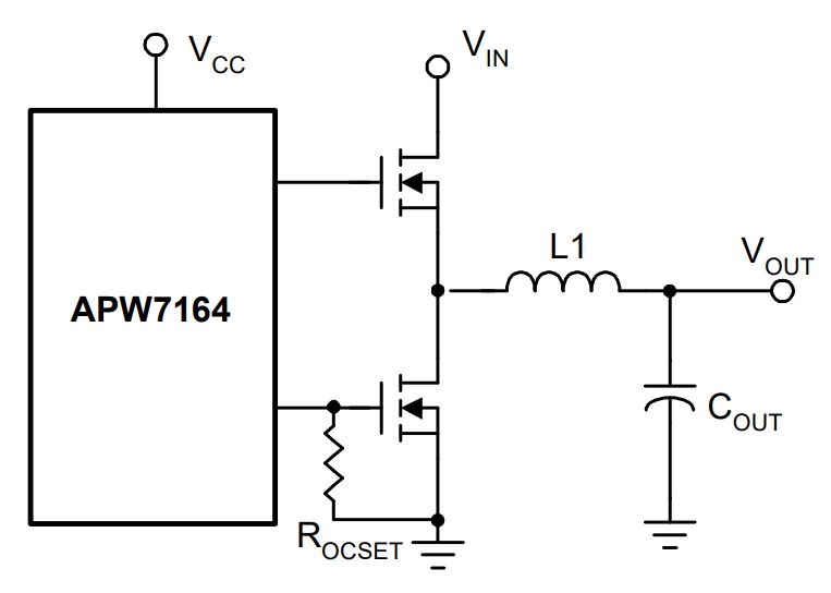
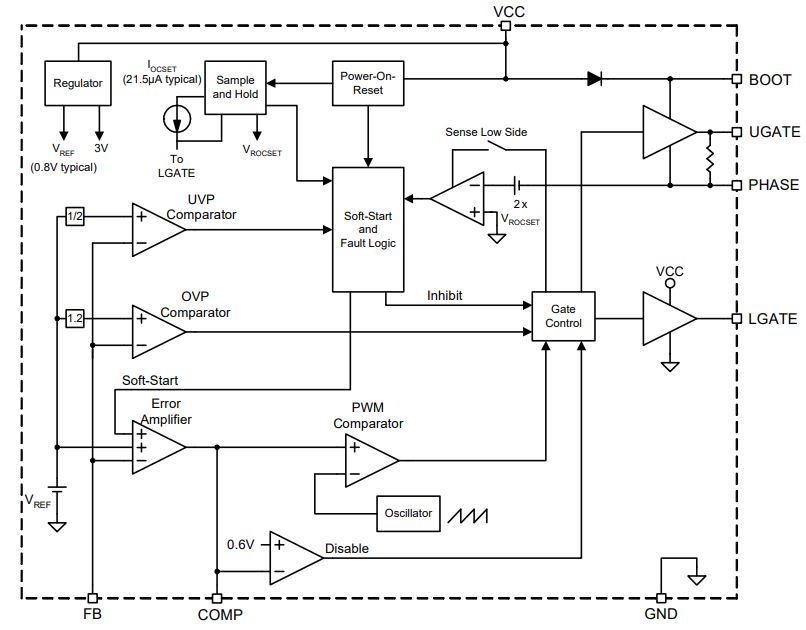
APW7164
Active
Synchronous Buck Controller
Features
- ±1% Over Line Voltage and Temperature Range
General Description
The APW7164 is a voltage mode, fixed 200kHz-switching frequency, synchronous buck converter. The APW7164 allows wide input voltage that is either a single 12V or two supply voltage(s) for various applications. A Power-On-Reset (POR) circuit monitors the VCC supply voltage to prevent wrong logic controls. A built-in digital soft-start circuit prevents the output voltages from overshoot as well as limits the input current. An internal 0.8V temperature-compensated reference voltage with high accuracy is designed to meet the requirement of low output voltage applications. The APW7164 provides excellent output voltage regulations against load current variation. The controller’s over-current protection monitors the output current by using the voltage drop across the RDS(ON) of low-side MOSFET, eliminating the need for a current sensing resistor that features high efficiency and low cost. The APW7164 also integrate over-voltage protection (OVP) and under-voltage protection (UVP) circuits which monitor the FB voltage to prevent the PWM output from over voltage and under voltage. The APW7164 is available in a simple SOP-8 package.
Features
- Excellent Reference Voltage Regulations
- ±1% Over Line Voltage and Temperature Range
- Integrated Soft-Start
- Fixed 200kHz Operation Frequency
- Voltage Mode PWM Operation with Up to 90% (Max.) Duty Cycle
- Under-Voltage Protection
- Adjustable Over-Current Protection Threshold
- Over-Voltage Protection
- Simple SOP-8 Package
- Lead Free and Green Devices Available (RoHS Compliant)
General Description
The APW7164 is a voltage mode, fixed 200kHz-switching frequency, synchronous buck converter. The APW7164 allows wide input voltage that is either a single 12V or two supply voltage(s) for various applications. A Power-On-Reset (POR) circuit monitors the VCC supply voltage to prevent wrong logic controls. A built-in digital soft-start circuit prevents the output voltages from overshoot as well as limits the input current. An internal 0.8V temperature-compensated reference voltage with high accuracy is designed to meet the requirement of low output voltage applications. The APW7164 provides excellent output voltage regulations against load current variation. The controller’s over-current protection monitors the output current by using the voltage drop across the RDS(ON) of low-side MOSFET, eliminating the need for a current sensing resistor that features high efficiency and low cost. The APW7164 also integrate over-voltage protection (OVP) and under-voltage protection (UVP) circuits which monitor the FB voltage to prevent the PWM output from over voltage and under voltage. The APW7164 is available in a simple SOP-8 package.
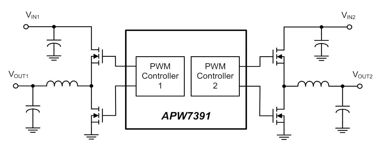
APW7391
Active
Dual Channel Synchronous Buck PWM Controller
Features
- Discontinuous Conduction Mode in Light Load to Increase Efficiency (VEN=2V)
- Sence External RSENSE (option 2)
General Description
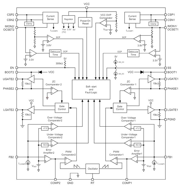
The APW7391 is a dual channel voltage mode, synchronous PWM controller which drives dual N-channel MOSFETs. The device integrates monitoring and protection functions into a single package, provides two controlled power output with under-voltage and overcurrent protections. The APW7391 provides excellent regulation for output load variation. The internal 1.0V temperature compensated reference voltage provides high accuracy of 0.8% over line and load regulation. The PWM switching frequency is adjustable from 50kHz to 350kHz. The APW7391 has been equipped with excellent protection functions: POR, IMON, OCP, SCP, UVP, OVP OTP. The Power-On-Reset (POR) circuit can monitor the VCC input voltage to make sure the supply voltage is valid. The APW7391 adopts either the external power inductor’s DCR or an external accurate sense resistor to sense the output current. The output current information is reported at IMON pin whose output voltage is proportional to output current. During the PWM switching, the APW7391 has OCP and SCP protections. When the load current exceeds the OCP or SCP threshold, the APW7391 shuts off its PWM switcher to prevent catastrophic failure caused by abnormal load or short-circuit. The APW7391 senses its FB pin for output UVP and OVP protection, which is 50% and 120% of reference voltage respectively. When the UVP or OVP occurs, the APW7391 latches off the PWM switcher. APW7391 has over temperature protection. When the die temperature is above 150°C, the APW7391 ceases PWM operation and recover normal operation when the die temperature drops by 40°C. The APW7391 is available in SSOP-24 and SSOP-24P packages, which is compliant with RoHS.
Features
- Single 12V Power Supply Required
- Excellent Output Voltage Regulation
- Simple Single Loop Control Design
- Programmable Frequency Range from 50kHz ~ 350kHz
- CCM/DCM Operation Selectable by EN Pin
- Discontinuous Conduction Mode in Light Load to Increase Efficiency (VEN=2V)
- Output Current Monitor (IMON Pin)
- Integrated Soft-Start and Soft-Off
- Support Pre-Biased Power-On
- Output Power Line Compensation
- Phase Shift 180°
- Integrated Boot-Strap Diode
- Over-Current and Short-Circuit Protection
- Sence External RSENSE (option 2)
- 120% Over-Voltage Protection
- 50% Under-Voltage Protection
- Over-Temperature Protection
- Available in SSOP-24 and SSOP-24P Packages
General Description
The APW7391 is a dual channel voltage mode, synchronous PWM controller which drives dual N-channel MOSFETs. The device integrates monitoring and protection functions into a single package, provides two controlled power output with under-voltage and overcurrent protections. The APW7391 provides excellent regulation for output load variation. The internal 1.0V temperature compensated reference voltage provides high accuracy of 0.8% over line and load regulation. The PWM switching frequency is adjustable from 50kHz to 350kHz. The APW7391 has been equipped with excellent protection functions: POR, IMON, OCP, SCP, UVP, OVP OTP. The Power-On-Reset (POR) circuit can monitor the VCC input voltage to make sure the supply voltage is valid. The APW7391 adopts either the external power inductor’s DCR or an external accurate sense resistor to sense the output current. The output current information is reported at IMON pin whose output voltage is proportional to output current. During the PWM switching, the APW7391 has OCP and SCP protections. When the load current exceeds the OCP or SCP threshold, the APW7391 shuts off its PWM switcher to prevent catastrophic failure caused by abnormal load or short-circuit. The APW7391 senses its FB pin for output UVP and OVP protection, which is 50% and 120% of reference voltage respectively. When the UVP or OVP occurs, the APW7391 latches off the PWM switcher. APW7391 has over temperature protection. When the die temperature is above 150°C, the APW7391 ceases PWM operation and recover normal operation when the die temperature drops by 40°C. The APW7391 is available in SSOP-24 and SSOP-24P packages, which is compliant with RoHS.
APW8723B
Active
5V to 12V Single Buck Voltage Mode PWM Controller
Features
- ±1% Over Temperature Range
General Description
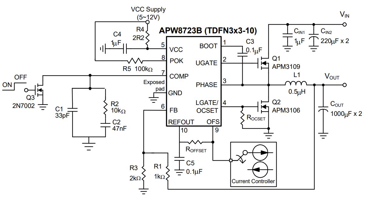
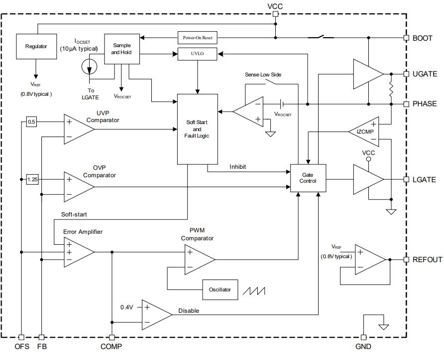
The APW8723B is a voltage mode, fixed 300kHz switching frequency, synchronous buck converter. The APW8723B allows wide input voltage that is either a single 5V~12V or two supply voltage(s) for various applications. The power-on-reset (POR) circuit monitors the VCC supply voltage to prevent wrong logic controls. A built-in soft-start circuit prevents the output voltages from overshoot as well as limits the input current. An internal 0.8V temperature compensated reference voltage with high accuracy is designed to meet the requirement of low output voltage applications. The APW8723B provides excellent output voltage regulations against load current variation. APW8723B is built in reference voltage offset function for applications that require adjusting supply voltage. The controller’s over-current protection monitors the output current by using the voltage drop across the RDS(ON) of low-side MOSFET, eliminating the need for a current sensing resistor that features high efficiency and low cost. In addition, the APW8723B also integrates excellent protection functions, the over-voltage protection (OVP) , under-voltage protection (UVP) and over-temperature protection (OTP). OVP circuit which monitors the FB voltage to prevent the PWM output from over voltage, and UVP circuit which monitors the FB voltage to prevent the PWM output from under voltage or short circuit. OTP circuit which monitors the junction temperature to prevent over-heating conditions. The APW8723B is available in TDFN3x3-10 package.
Features
- Wide 5V to 12V Supply Voltage
- Power-On-Reset Monitoring on VCC
- Excellent Output Voltage Regulations
- ±1% Over Temperature Range
- Integrated Soft-Start
- Voltage Mode PWM Operation with External Compensation
- Up to 90%Duty Ratio for Fast Transient Response
- Constant Switching Frequency
- Integrated Bootstrap Forward P-CH MOSFET
- Drive Dual Low Cost N-MOSFETs with Adaptive Dead Time Control
- 50% Under-Voltage Protection
- 125% Over-Voltage Protection
- Adjustable Over-Current Protection Threshold
- Shutdown Control by COMP
- Power Good Monitoring
- TDFN3x3-10 Package
General Description
The APW8723B is a voltage mode, fixed 300kHz switching frequency, synchronous buck converter. The APW8723B allows wide input voltage that is either a single 5V~12V or two supply voltage(s) for various applications. The power-on-reset (POR) circuit monitors the VCC supply voltage to prevent wrong logic controls. A built-in soft-start circuit prevents the output voltages from overshoot as well as limits the input current. An internal 0.8V temperature compensated reference voltage with high accuracy is designed to meet the requirement of low output voltage applications. The APW8723B provides excellent output voltage regulations against load current variation. APW8723B is built in reference voltage offset function for applications that require adjusting supply voltage. The controller’s over-current protection monitors the output current by using the voltage drop across the RDS(ON) of low-side MOSFET, eliminating the need for a current sensing resistor that features high efficiency and low cost. In addition, the APW8723B also integrates excellent protection functions, the over-voltage protection (OVP) , under-voltage protection (UVP) and over-temperature protection (OTP). OVP circuit which monitors the FB voltage to prevent the PWM output from over voltage, and UVP circuit which monitors the FB voltage to prevent the PWM output from under voltage or short circuit. OTP circuit which monitors the junction temperature to prevent over-heating conditions. The APW8723B is available in TDFN3x3-10 package.
APW8731C
Active
Dual-Phase COT Buck PWM Controller
Features
General Description
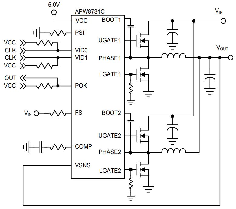
The APW8731C is a dual-phase PWM control IC which provides a precision voltage regulation system and supports wide input range from 5.4V to 24V. By integrating dual-phase power MOSFET drivers and controller into the one IC, APW8731C can reduce the number of external components for a cost and space saving power management solution. The APW8731C's PWM controller adopts constant on time architecture which has the trait of excellent transient resposnse. The PWM controller features automatic phase reduction that can either operates in dual-phase mode or single-phase mode, depending on resistor settings on PSI and LGATE2 pin. The resistor on LGATE2 pin can also set PWM/PFM/USM operations. The device integrates adjustable load line voltage positioning (droop) and detect voltage on low side RDS(ON) for channel-current balance. The protection functions include over current protection (OCP), under voltage protection (UVP), over voltage protection (OVP) and over temperature protection (OTP). OCP, UVP or OVP occurrence will lead to latch-off. A thermal shutdown function is implemented to prevent damages due to heat by excessive power dissipation. Typically the thermal shutdown threshold temperature is 150oC. When the thermal shutdown is triggered the device stops switching and output voltage re-start after the junction temperature cools by 30oC. APW8731C is packaged in TQFN 4x4-24.
Features
- Support Wide Input Voltage Range from 5.4V to 24V
- VCC Support Range from 4.5V to 5.5V
- Integrated High-Side MOSFET Driver with Integrated Bootstrap P-CHMOSFET
- Drive N-CH MOSFET with built in Adaptive Dead Time Control Scheme
- Support Single-PFM, Two Phase PWM, and Ultra-Sonic PFM Mode
- PWM Switching Frequency 500kHz ~700kHz by FS Pin
- Built In Constant On Time PWM Control with Current Balance Operation
- Support Single and Two Phase PWM Control by LGATE2 & PSI Voltage Setting
- Built In Adjustable Over Current Protection by LGATE1 Setting
- Built In Under Voltage Protection with Latch Off Mode
- Built In Over Voltage Protection with Latch Off Mode
- Built In Over Temperature Protection
- Individual EN & POK Indicator
- Built In VID for VOUT Adjustment
- Built In Decay Down Mode
- TQFN 4x4-24 Package
General Description
The APW8731C is a dual-phase PWM control IC which provides a precision voltage regulation system and supports wide input range from 5.4V to 24V. By integrating dual-phase power MOSFET drivers and controller into the one IC, APW8731C can reduce the number of external components for a cost and space saving power management solution. The APW8731C's PWM controller adopts constant on time architecture which has the trait of excellent transient resposnse. The PWM controller features automatic phase reduction that can either operates in dual-phase mode or single-phase mode, depending on resistor settings on PSI and LGATE2 pin. The resistor on LGATE2 pin can also set PWM/PFM/USM operations. The device integrates adjustable load line voltage positioning (droop) and detect voltage on low side RDS(ON) for channel-current balance. The protection functions include over current protection (OCP), under voltage protection (UVP), over voltage protection (OVP) and over temperature protection (OTP). OCP, UVP or OVP occurrence will lead to latch-off. A thermal shutdown function is implemented to prevent damages due to heat by excessive power dissipation. Typically the thermal shutdown threshold temperature is 150oC. When the thermal shutdown is triggered the device stops switching and output voltage re-start after the junction temperature cools by 30oC. APW8731C is packaged in TQFN 4x4-24.
APW8828
Active
High-Performance Notebook PWM Controller
Features
± 1% Accuracy Over-Temperature
General Description
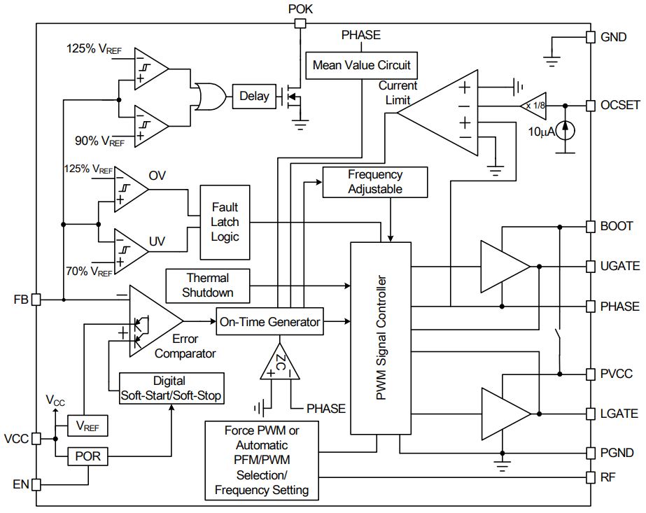
The APW8828 is a single-phase, constant-on-time, synchronous PWM controller, which drives N-channel MOSFETs. The APW8828 steps down high voltage to generate low-voltage for chipset or RAM supplies in notebook computers. The APW8828 provides excellent transient response and accurate DC voltage output in either PFM or PWM Mode. In Pulse Frequency Mode (PFM), the APW8828 provides very high efficiency over light to heavy loads with loadingmodulated switching frequencies. In PWM Mode, the converter works nearly at constant frequency for low-noise requirements. The APW8828 is equipped with accurate positive currentlimit, output under-voltage, and output over-voltage protections, perfect for NB applications. The Power-OnReset function monitors the voltage on VCC to prevent wrong operation during power-on. The APW8828 has a 1ms digital soft-start and integrates ramp-down control for soft-stop. An internal integrated soft-start ramps up the output voltage with programmable slew rate to reduce the start-up current. A soft-stop function actively discharges the output capacitors with controlled reverse inductor current. The APW8828 is available in 10pin TDFN 3x3 package.
Features
- Adjustable Output Voltage from +0.7V to +5.5V
± 1% Accuracy Over-Temperature
- Operates from an Input Battery Voltage Range of +1.8V to +28V
- Power-On-Reset Monitoring on VCC Pin
- Excellent Line and Load Transient Responses
- PFM Mode for Increased Light Load Efficiency
- Selectable PWM Frequency from 4 Preset Values
- Integrated MOSFET Drivers
- Integrated Bootstrap Forward P-CH MOSFET
- Adjustable Integrated Soft-Start and Soft-Stop
- Selectable Forced PWM or Automatic PFM/PWM Mode
- Power Good Monitoring
- 70% Under-Voltage Protection
- 125% Over-Voltage Protection
- Adjustable Current-Limit Protection
- Over-Temperature Protection
- TDFN-10 3x3 Package
- Lead Free and Green Devices Available (RoHS Compliant)
General Description
The APW8828 is a single-phase, constant-on-time, synchronous PWM controller, which drives N-channel MOSFETs. The APW8828 steps down high voltage to generate low-voltage for chipset or RAM supplies in notebook computers. The APW8828 provides excellent transient response and accurate DC voltage output in either PFM or PWM Mode. In Pulse Frequency Mode (PFM), the APW8828 provides very high efficiency over light to heavy loads with loadingmodulated switching frequencies. In PWM Mode, the converter works nearly at constant frequency for low-noise requirements. The APW8828 is equipped with accurate positive currentlimit, output under-voltage, and output over-voltage protections, perfect for NB applications. The Power-OnReset function monitors the voltage on VCC to prevent wrong operation during power-on. The APW8828 has a 1ms digital soft-start and integrates ramp-down control for soft-stop. An internal integrated soft-start ramps up the output voltage with programmable slew rate to reduce the start-up current. A soft-stop function actively discharges the output capacitors with controlled reverse inductor current. The APW8828 is available in 10pin TDFN 3x3 package.
APW8828K
Active
High-Performance Notebook PWM Controller
Features
- ±1% Accuracy Over-Temperature
General Description
The APW8828K is a single-phase, constant-on-time, synchronous PWM controller, which drives N-channel MOSFETs. The APW8828K steps down high voltage to generate low-voltage for chipset or RAM supplies in notebook computers. The APW8828K provides excellent transient response and accurate DC voltage output in either PFM or PWM Mode. In Pulse Frequency Mode (PFM), the APW8828K provides very high efficiency over light to heavy loads with loading-modulated switching frequencies. In PWM Mode, the converter works nearly at constant frequency for lownoise requirements. The APW8828K is equipped with accurate positive current-limit, output under-voltage, and output overvoltage protections, perfect for NB applications. The Power-On-Reset function monitors the voltage on VCC to prevent wrong operation during power-on. The APW8828K has a 1ms digital soft-start and integrates ramp-down control for soft-stop. An internal integrated soft-start ramps up the output voltage with programmable slew rate to reduce the start-up current. A soft-stop function actively discharges the output capacitors with controlled reverse inductor current. The APW8828K is available in 16pin TQFN 3x3 package.
Features
- Adjustable Output Voltage from +0.7V to +5.5V
- ±1% Accuracy Over-Temperature
- Operates from an Input Battery Voltage Range of +1.8V to +28V
- Power-On-Reset Monitoring on VCC Pin
- Excellent Line and Load Transient Responses
- PFM Mode for Increased Light Load Efficiency
- Selectable PWM Frequency from 4 Preset Values
- Integrated MOSFET Drivers
- Integrated Bootstrap Forward P-CH MOSFET
- Adjustable Integrated Soft-Start and Soft-Stop
- Selectable Forced PWM or Automatic PFM/PWM Mode
- Power Good Monitoring
- 70% Under-Voltage Protection
- 125% Over-Voltage Protection
- Adjustable Current-Limit Protection
- Over-Temperature Protection
- TQFN-16 3x3 Package
General Description
The APW8828K is a single-phase, constant-on-time, synchronous PWM controller, which drives N-channel MOSFETs. The APW8828K steps down high voltage to generate low-voltage for chipset or RAM supplies in notebook computers. The APW8828K provides excellent transient response and accurate DC voltage output in either PFM or PWM Mode. In Pulse Frequency Mode (PFM), the APW8828K provides very high efficiency over light to heavy loads with loading-modulated switching frequencies. In PWM Mode, the converter works nearly at constant frequency for lownoise requirements. The APW8828K is equipped with accurate positive current-limit, output under-voltage, and output overvoltage protections, perfect for NB applications. The Power-On-Reset function monitors the voltage on VCC to prevent wrong operation during power-on. The APW8828K has a 1ms digital soft-start and integrates ramp-down control for soft-stop. An internal integrated soft-start ramps up the output voltage with programmable slew rate to reduce the start-up current. A soft-stop function actively discharges the output capacitors with controlled reverse inductor current. The APW8828K is available in 16pin TQFN 3x3 package.
APW8833A
Active
System Power PWM Controller with Economy Standby Mode
Features
- PWM2 Controller with Adjustable (2V to 5.5V) Output
- 100mA Low Dropout Regulator (LDO5) with Fixed 5V Output
- 100mA Low Dropout Regulator (LDO3) with Fixed 3.3V Output
- 250kHz Clock Signal for 15V Charge Pump (Used PWM1 as Its Power Supply)
General Description
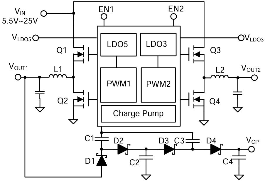
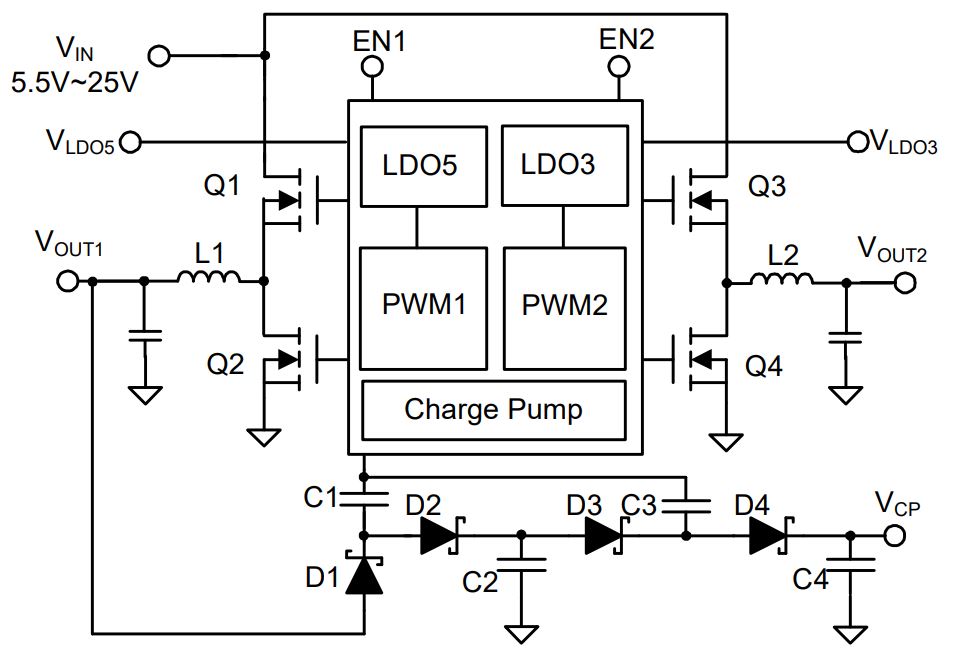
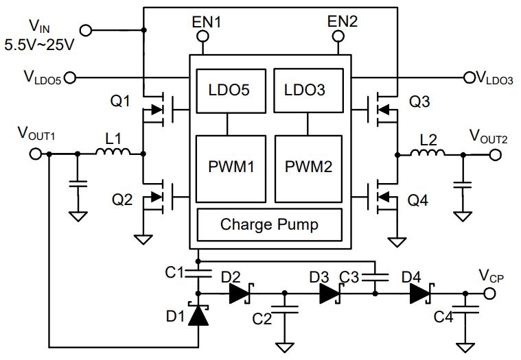
The APW8833A integrates dual step-down, constant-ontime, synchronous PWM controllers (that drives dual Nchannel MOSFETs for each channel) and two low dropout regulators as well as various protections into a chip. The PWM controllers step down high voltage of a battery to generate low-voltage for NB applications. The output of PWM1 and PWM2 can be adjusted from 2V to 5.5V by setting a resistive voltage-divider from VOUTx to GND. The linear regulators provide 5V and 3.3V output for standby power supply. The linear regulators provide up to 100mA output current. When the PWMx output voltage is higher than LDOx bypass threshold, the related LDOx regulator is shut off and its output is connected to VOUTx by internal switchover MOSFET. It can save power dissipation. The charge pump circuit with 250kHz clock driver uses VOUT1 as its power supply to generate approximately 15V DC voltage. The APW8833A provides excellent transient response and accurate DC output voltage in either PFM or PWM Mode. In Pulse-Frequency Mode (PFM), the APW8833A provides very high efficiency over light to heavy loads with loadingmodulated switching frequencies. The Forced-PWM Mode works nearly at constant frequency for low-noise requirements. The unique ultrasonic mode maintains the switching frequency above 25kHz, which eliminates noise in audio application. The APW8833A has individual enable controls for each PWM channels. Pulling both EN1/2 pin low shuts down the all of outputs. The LDO3 and LDO5 of APW8833A are always on standby power.The APW8833A is available in a TQFN3x3-20 package.
Features
- Wide Input Voltage Range from 5.5V to 25V
- Provide 5 Independent Outputs with ±1.0% Accuracy Over-Temperature
- PWM2 Controller with Adjustable (2V to 5.5V) Output
- 100mA Low Dropout Regulator (LDO5) with Fixed 5V Output
- 100mA Low Dropout Regulator (LDO3) with Fixed 3.3V Output
- 250kHz Clock Signal for 15V Charge Pump (Used PWM1 as Its Power Supply)
- Excellent Line/Load Regulations about ±1.5% Over-Temperature Range at PWM Channels
- Low Consumption in Standby Mode
- 2Cells Input Battery Support
- Built in POR Control Scheme Implemented
- Constant On-Time Control Scheme
- Built in Soft Start for PWM Outputs and Soft Stop for PWM Outputs and LDO Outputs
- Integrated Bootstrap Forward P-CH MOSFET
- High Efficiency over Light to Full Load Range (PWMs)
- Built in Power Good Indicators (PWMs)
- 60% Under-Voltage and 115% Over-Voltage Protections (PWM)
- Adjustable Current-Limit Protection (PWMs)
- Over-Temperature Protection
- 3mmx3mm Thin QFN-20 (TQFN3x3-20) Package
- Lead Free and Green Device Available (RoHS Compliant)
General Description
The APW8833A integrates dual step-down, constant-ontime, synchronous PWM controllers (that drives dual Nchannel MOSFETs for each channel) and two low dropout regulators as well as various protections into a chip. The PWM controllers step down high voltage of a battery to generate low-voltage for NB applications. The output of PWM1 and PWM2 can be adjusted from 2V to 5.5V by setting a resistive voltage-divider from VOUTx to GND. The linear regulators provide 5V and 3.3V output for standby power supply. The linear regulators provide up to 100mA output current. When the PWMx output voltage is higher than LDOx bypass threshold, the related LDOx regulator is shut off and its output is connected to VOUTx by internal switchover MOSFET. It can save power dissipation. The charge pump circuit with 250kHz clock driver uses VOUT1 as its power supply to generate approximately 15V DC voltage. The APW8833A provides excellent transient response and accurate DC output voltage in either PFM or PWM Mode. In Pulse-Frequency Mode (PFM), the APW8833A provides very high efficiency over light to heavy loads with loadingmodulated switching frequencies. The Forced-PWM Mode works nearly at constant frequency for low-noise requirements. The unique ultrasonic mode maintains the switching frequency above 25kHz, which eliminates noise in audio application. The APW8833A has individual enable controls for each PWM channels. Pulling both EN1/2 pin low shuts down the all of outputs. The LDO3 and LDO5 of APW8833A are always on standby power.The APW8833A is available in a TQFN3x3-20 package.
APW8833/B
Active
System Power PWM Controller with Economy Standby Mode
Features
- PWM2 Controller with Adjustable (2V to 5.5V) Output
- 100mA Low Dropout Regulator (LDO5) with Fixed 5V Output
- 100mA Low Dropout Regulator (LDO3) with Fixed 3.3V Output
- 250kHz Clock Signal for 15V Charge Pump (Used PWM1 as Its Power Supply)
General Description
The APW8833 integrates dual step-down, constant-ontime, synchronous PWM controllers (that drives dual Nchannel MOSFETs for each channel) and two low dropout regulators as well as various protections into a chip. The PWM controllers step down high voltage of a battery to generate low-voltage for NB applications. The output of PWM1 and PWM2 can be adjusted from 2V to 5.5V by setting a resistive voltage-divider from VOUTx to GND. The linear regulators provide 5V and 3.3V output for standby power supply. The linear regulators provide up to 100mA output current. When the PWMx output voltage is higher than LDOx bypass threshold, the related LDOx regulator is shut off and its output is connected to VOUTx by internal switchover MOSFET. It can save power dissipation. The charge pump circuit with 250kHz clock driver uses VOUT1 as its power supply to generate approximately 15V DC voltage. The APW8833 provides excellent transient response and accurate DC output voltage in either PFM or PWM Mode. In Pulse-Frequency Mode (PFM), the APW8833 provides very high efficiency over light to heavy loads with load ingmodulated switching frequencies. The Forced-PWM Mode works nearly at constant frequency for low-noise requirements. The unique ultrasonic mode maintains the switching frequency above 25kHz, which eliminates noise in audio application. The APW8833 has individual enable controls for each PWM channels. Pulling both EN1/2 pin low shuts down the all of outputs. The LDO3 and LDO5 of APW8833 B/C are always on standby power. The APW8833 is available in a TQFN3x3-20 package.
Features
- Wide Input Voltage Range from 5.5V to 25V
- Provide 5 Independent Outputs with ±1.0% Accuracy Over-Temperature
- PWM2 Controller with Adjustable (2V to 5.5V) Output
- 100mA Low Dropout Regulator (LDO5) with Fixed 5V Output
- 100mA Low Dropout Regulator (LDO3) with Fixed 3.3V Output
- 250kHz Clock Signal for 15V Charge Pump (Used PWM1 as Its Power Supply)
- Excellent Line/Load Regulations about ±1.5% Over-Temperature Range at PWM Channels
- Low Consumption in Standby Mode
- 2Cells Input Battery Support
- Built In POR Control Scheme Implemented
- Constant On-Time Control Scheme
- Built In Soft Start for PWM Outputs and Soft Stop for PWM Outputs and LDO Outputs
- Integrated Bootstrap Forward P-CH MOSFET
- High Efficiency over Light to Full Load Range (PWMs)
- Built In Power Good Indicators (PWMs)
- 60% Under-Voltage and 115% Over-Voltage Protections (PWM)
- Adjustable Current-Limit Protection (PWMs)
- Over-Temperature Protection
- 3mmx3mm Thin QFN-20 (TQFN3x3-20) Package
- Lead Free and Green Device Available (RoHS Compliant)
General Description
The APW8833 integrates dual step-down, constant-ontime, synchronous PWM controllers (that drives dual Nchannel MOSFETs for each channel) and two low dropout regulators as well as various protections into a chip. The PWM controllers step down high voltage of a battery to generate low-voltage for NB applications. The output of PWM1 and PWM2 can be adjusted from 2V to 5.5V by setting a resistive voltage-divider from VOUTx to GND. The linear regulators provide 5V and 3.3V output for standby power supply. The linear regulators provide up to 100mA output current. When the PWMx output voltage is higher than LDOx bypass threshold, the related LDOx regulator is shut off and its output is connected to VOUTx by internal switchover MOSFET. It can save power dissipation. The charge pump circuit with 250kHz clock driver uses VOUT1 as its power supply to generate approximately 15V DC voltage. The APW8833 provides excellent transient response and accurate DC output voltage in either PFM or PWM Mode. In Pulse-Frequency Mode (PFM), the APW8833 provides very high efficiency over light to heavy loads with load ingmodulated switching frequencies. The Forced-PWM Mode works nearly at constant frequency for low-noise requirements. The unique ultrasonic mode maintains the switching frequency above 25kHz, which eliminates noise in audio application. The APW8833 has individual enable controls for each PWM channels. Pulling both EN1/2 pin low shuts down the all of outputs. The LDO3 and LDO5 of APW8833 B/C are always on standby power. The APW8833 is available in a TQFN3x3-20 package.
APW8833/C
Active
System Power PWM Controller with Economy Standby Mode
Features
- PWM2 Controller with Adjustable (2V to 5.5V) Output
- 100mA Low Dropout Regulator (LDO5) with Fixed 5V Output
- 100mA Low Dropout Regulator (LDO3) with Fixed 3.3V Output
- 250kHz Clock Signal for 15V Charge Pump (Used PWM1 as Its Power Supply)
General Description
The APW8833 integrates dual step-down, constant-ontime, synchronous PWM controllers (that drives dual Nchannel MOSFETs for each channel) and two low dropout regulators as well as various protections into a chip. The PWM controllers step down high voltage of a battery to generate low-voltage for NB applications. The output of PWM1 and PWM2 can be adjusted from 2V to 5.5V by setting a resistive voltage-divider from VOUTx to GND. The linear regulators provide 5V and 3.3V output for standby power supply. The linear regulators provide up to 100mA output current. When the PWMx output voltage is higher than LDOx bypass threshold, the related LDOx regulator is shut off and its output is connected to VOUTx by internal switchover MOSFET. It can save power dissipation. The charge pump circuit with 250kHz clock driver uses VOUT1 as its power supply to generate approximately 15V DC voltage. The APW8833 provides excellent transient response and accurate DC output voltage in either PFM or PWM Mode. In Pulse-Frequency Mode (PFM), the APW8833 provides very high efficiency over light to heavy loads with loadingmodulated switching frequencies. The Forced-PWM Mode works nearly at constant frequency for low-noise requirements. The unique ultrasonic mode maintains the switching frequency above 25kHz, which eliminates noise in audio application. The APW8833 has individual enable controls for each PWM channels. Pulling both EN1/2 pin low shuts down the all of outputs. The LDO3 and LDO5 of APW8833 B/C are always on standby power. The APW8833 is available in a TQFN3x3-20 package.
Features
- Wide Input voltage Range from 5.5V to 25V
- Provide 5 Independent Outputs with ±1.0% Accuracy Over-Temperature
- PWM2 Controller with Adjustable (2V to 5.5V) Output
- 100mA Low Dropout Regulator (LDO5) with Fixed 5V Output
- 100mA Low Dropout Regulator (LDO3) with Fixed 3.3V Output
- 250kHz Clock Signal for 15V Charge Pump (Used PWM1 as Its Power Supply)
- Excellent Line/Load Regulations about ±1.5% over-temperature range at PWM Channels
- Low Consumption in Standby Mode
- 2Cells Input Battery Support
- Built in POR Control Scheme Implemented
- Constant On-Time Control Scheme
- Built in Soft Start for PWM Outputs and Soft Stop for PWM Outputs and LDO Outputs
- Integrated Bootstrap Forward P-CH MOSFET
- High Efficiency over Light to Full Load Range (PWMs)
- Built in Power Good Indicators (PWMs)
- 60% Under-Voltage and 115% Over-Voltage Protections (PWM)
- Adjustable Current-Limit Protection (PWMs)
- Over-Temperature Protection
- 3mmx3mm Thin QFN-20 (TQFN3x3-20) package
- Lead Free and Green Device Available (RoHS Compliant)
General Description
The APW8833 integrates dual step-down, constant-ontime, synchronous PWM controllers (that drives dual Nchannel MOSFETs for each channel) and two low dropout regulators as well as various protections into a chip. The PWM controllers step down high voltage of a battery to generate low-voltage for NB applications. The output of PWM1 and PWM2 can be adjusted from 2V to 5.5V by setting a resistive voltage-divider from VOUTx to GND. The linear regulators provide 5V and 3.3V output for standby power supply. The linear regulators provide up to 100mA output current. When the PWMx output voltage is higher than LDOx bypass threshold, the related LDOx regulator is shut off and its output is connected to VOUTx by internal switchover MOSFET. It can save power dissipation. The charge pump circuit with 250kHz clock driver uses VOUT1 as its power supply to generate approximately 15V DC voltage. The APW8833 provides excellent transient response and accurate DC output voltage in either PFM or PWM Mode. In Pulse-Frequency Mode (PFM), the APW8833 provides very high efficiency over light to heavy loads with loadingmodulated switching frequencies. The Forced-PWM Mode works nearly at constant frequency for low-noise requirements. The unique ultrasonic mode maintains the switching frequency above 25kHz, which eliminates noise in audio application. The APW8833 has individual enable controls for each PWM channels. Pulling both EN1/2 pin low shuts down the all of outputs. The LDO3 and LDO5 of APW8833 B/C are always on standby power. The APW8833 is available in a TQFN3x3-20 package.

APW8868B
Active
DDR2 and DDR3/DDR3L Synchronous Buck Controller With 1.5A LDO Support Low IQ & DROOP
Features
Buck Controller (VDDQ)
- Adjustable Switching Frequency from 400kHz to 550kHz in PWM Mode with DC Output Current
General Description
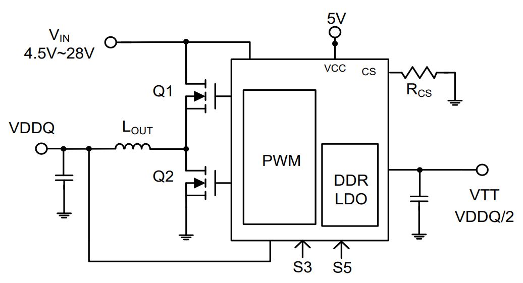
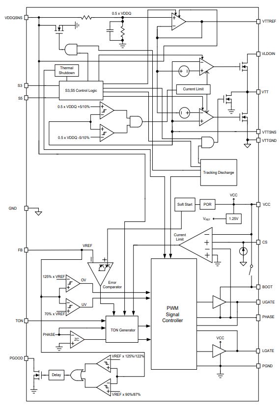
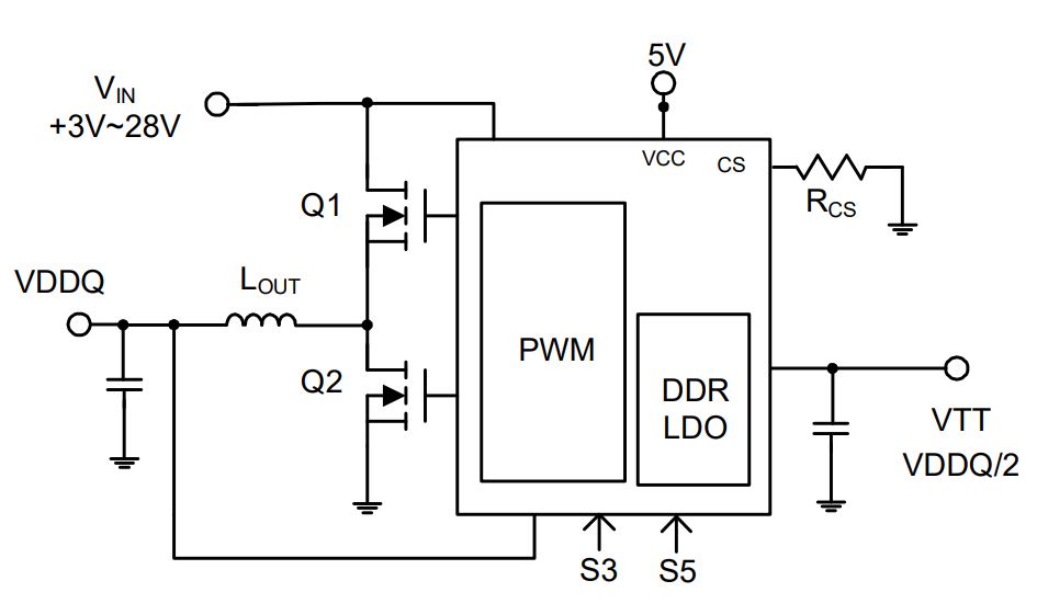
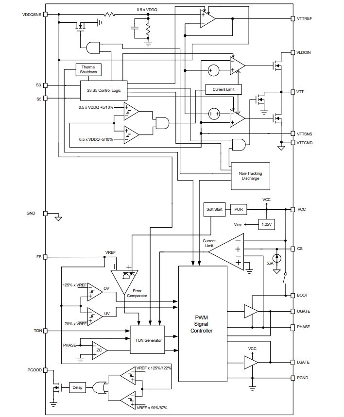
The APW8868B integrates a synchronous buck PWM controller to generate VDDQ, a sourcing and sinking LDO linear regulator to generate VTT. It offers the lowest total solution cost in system where space is at a premium. The APW8868B provides excellent transient response and accurate DC voltage output in either PFM or PWM Mode. In Pulse Frequency Mode (PFM), the APW8868B provides very high efficiency over light to heavy loads with loading-modulated switching frequencies. On TQFN-20 Package, the Forced PWM Mode works nearly at constant frequency for low-noise requirements. The APW8868B is equipped with accurate current-limit, output under-voltage, and output over-voltage protections. A Power-On- Reset function monitors the voltage on VCC prevents wrong operation during power on. The LDO is designed to provide a regulated voltage with bi-directional output current for DDR-SDRAM termination. The device integrates two power transistors to source or sink current up to 1.5A. It also incorporates current-limit and thermal shutdown protection. The output voltage of LDO tracks the voltage at VREF pin. An internal resistor divider is used to provide a half voltage of VREF for VTTREF and VTT Voltage. The VTT output voltage is only requiring 20µF of ceramic output capacitance for stability and fast transient response. The S3 and S5 pins provide the sleep state for VTT (S3 state) and suspend state (S4/S5 state) for device, when S5 and S3 are both pulled low the device provides the soft-off for VTT and VTTREF.
Features
Buck Controller (VDDQ)
- High Input Voltages Range from 3V to 28V Input Power
- Provide Adjustable Output Voltage from 0.675V to 5.5V ±1% Accuracy Over Temperature
- Integrated MOSFET Drivers and Bootstrap Forward P-CHMOSFET
- Low Quiescent Current (200µA)
- Excellent Line and Load Transient Responses
- PFM Mode for Increased Light Load Efficiency
- Constant On-Time Controller Scheme
- Adjustable Switching Frequency from 400kHz to 550kHz in PWM Mode with DC Output Current
- S3 and S5 Pins Control The Device in S0, S3 or S4/ S5 State
- Power Good Monitoring
- 70% Under-Voltage Protection (UVP)
- 125% Over-Voltage Protection (OVP)
- Adjustable Current-Limit Protection
- TQFN-20 3mmx3mm Thin Package
- Lead Free Available (RoHS Compliant) ±1.5A LDO Section (VTT)
- Sourcing or Sinking Current Up to 1.5A
- Fast Transient Response for Output Voltage
- Output Ceramic Capacitors Support at Least 10µF MLCC
- VTT and VTTREF Track at Half the VDDQSNS by Internal Divider
- ±20mV Accuracy for VTT and VTTREF
- Independent Over-Current Limit (OCL)
- Thermal Shutdown Protection
General Description
The APW8868B integrates a synchronous buck PWM controller to generate VDDQ, a sourcing and sinking LDO linear regulator to generate VTT. It offers the lowest total solution cost in system where space is at a premium. The APW8868B provides excellent transient response and accurate DC voltage output in either PFM or PWM Mode. In Pulse Frequency Mode (PFM), the APW8868B provides very high efficiency over light to heavy loads with loading-modulated switching frequencies. On TQFN-20 Package, the Forced PWM Mode works nearly at constant frequency for low-noise requirements. The APW8868B is equipped with accurate current-limit, output under-voltage, and output over-voltage protections. A Power-On- Reset function monitors the voltage on VCC prevents wrong operation during power on. The LDO is designed to provide a regulated voltage with bi-directional output current for DDR-SDRAM termination. The device integrates two power transistors to source or sink current up to 1.5A. It also incorporates current-limit and thermal shutdown protection. The output voltage of LDO tracks the voltage at VREF pin. An internal resistor divider is used to provide a half voltage of VREF for VTTREF and VTT Voltage. The VTT output voltage is only requiring 20µF of ceramic output capacitance for stability and fast transient response. The S3 and S5 pins provide the sleep state for VTT (S3 state) and suspend state (S4/S5 state) for device, when S5 and S3 are both pulled low the device provides the soft-off for VTT and VTTREF.
APW8868C
Active
DDR2 and DDR3/DDR3L Synchronous Buck Controller With 1.5A LDO Support LOW IQ
Features
Buck Controller (VDDQ)
- Adjustable Switching Frequency from 400kHz to 550kHz in PWM Mode with DC Output Current
General Description
The APW8868C integrates a synchronous buck PWM controller to generate VDDQ, a sourcing and sinking LDO linear regulator to generate VTT. It offers the lowest total solution cost in system where space is at a premium. The APW8868C provides excellent transient response and accurate DC voltage output in either PFM or PWM Mode. In Pulse Frequency Mode (PFM), the APW8868C provides very high efficiency over light to heavy loads with loadingmodulated switching frequencies. On TQFN-20 Package, the Forced PWM Mode works nearly at constant frequency for low-noise requirements. The APW8868C is equipped with accurate current-limit, output under-voltage, and output over-voltage protections. A Power-On-Reset function monitors the voltage on VCC prevents wrong operation during power on. The LDO is designed to provide a regulated voltage with bi-directional output current for DDR-SDRAM termination. The device integrates two power transistors to source or sink current up to 1.5A. It also incorporates current-limit and thermal shutdown protection. The output voltage of LDO tracks the voltage at VREF pin. An internal resistor divider is used to provide a half voltage of VREF for VTTREF and VTT Voltage. The VTT output voltage is only requiring 20µF of ceramic output capacitance for stability and fast transient response. The S3 and S5 pins provide the sleep state for VTT (S3 state) and suspend state (S4/S5 state) for device, when S5 and S3 are both pulled low the device provides the soft-off for VTT and VTTREF.
Features
Buck Controller (VDDQ)
- High Input Voltages Range from 3V to 28V Input Power
- Provide Adjustable Output Voltage from 0.75V to 5.5V ±1% Accuracy Over Temperature
- Integrated MOSFET Drivers and Bootstrap Forward P-CH MOSFET
- Low Quiescent Current (200µA)
- Excellent Line and Load Transient Responses
- PFM Mode for Increased Light Load Efficiency
- Constant On-Time Controller Scheme
- Adjustable Switching Frequency from 400kHz to 550kHz in PWM Mode with DC Output Current
- S3 and S5 Pins Control The Device in S0, S3 or S4/ S5 State
- Power Good Monitoring
- 70% Under-Voltage Protection (UVP)
- 125% Over-Voltage Protection (OVP)
- Adjustable Current-Limit Protection
- TQFN-20 3mmx3mm Thin Package
- Lead Free Available (RoHS Compliant) ±1.5A LDO Section (VTT)
- Sourcing or Sinking Current Up to 1.5A
- Fast Transient Response for Output Voltage
- Output Ceramic Capacitors Support at Least 10mF MLCC
- VTT and VTTREF Track at Half the VDDQSNS by Internal Divider
- ±20mV Accuracy for VTT and VTTREF
- Independent Over-Current Limit (OCL)
- Thermal Shutdown Protection
General Description
The APW8868C integrates a synchronous buck PWM controller to generate VDDQ, a sourcing and sinking LDO linear regulator to generate VTT. It offers the lowest total solution cost in system where space is at a premium. The APW8868C provides excellent transient response and accurate DC voltage output in either PFM or PWM Mode. In Pulse Frequency Mode (PFM), the APW8868C provides very high efficiency over light to heavy loads with loadingmodulated switching frequencies. On TQFN-20 Package, the Forced PWM Mode works nearly at constant frequency for low-noise requirements. The APW8868C is equipped with accurate current-limit, output under-voltage, and output over-voltage protections. A Power-On-Reset function monitors the voltage on VCC prevents wrong operation during power on. The LDO is designed to provide a regulated voltage with bi-directional output current for DDR-SDRAM termination. The device integrates two power transistors to source or sink current up to 1.5A. It also incorporates current-limit and thermal shutdown protection. The output voltage of LDO tracks the voltage at VREF pin. An internal resistor divider is used to provide a half voltage of VREF for VTTREF and VTT Voltage. The VTT output voltage is only requiring 20µF of ceramic output capacitance for stability and fast transient response. The S3 and S5 pins provide the sleep state for VTT (S3 state) and suspend state (S4/S5 state) for device, when S5 and S3 are both pulled low the device provides the soft-off for VTT and VTTREF.
APW8869A
Active
DDR2 AND DDR3/DDR3L SYNCHRONOUS BUCK CONTROLLER WITH 1.5A LDO SUPPORT LOW IQ
Features
Buck Controller (VDDQ)
- Adjustable Switching Frequency from 400kHz to 550kHz in PWM Mode with DC Output Current
General Description
The APW8869A integrates a synchronous buck PWM controller to generate VDDQ, a sourcing and sinking LDO linear regulator to generate VTT. It offers the lowest total solution cost in system where space is at a premium. The APW8869A provides excellent transient response and accurate DC voltage output in either PFM or PWM Mode. In Pulse Frequency Mode (PFM), the APW8869A provides very high efficiency over light to heavy loads with loadingmodulated switching frequencies. On TQFN-20 Package, the Forced PWM Mode works nearly at constant frequency for low-noise requirements. The APW8869A is equipped with accurate current-limit, output under-voltage, and output over-voltage protections. A Power-On- Reset function monitors the voltage on VCC prevents wrong operation during power on. The LDO is designed to provide a regulated voltage with bi-directional output current for DDR-SDRAM termination. The device integrates two power transistors to source or sink current up to 1.5A. It also incorporates current-limit and thermal shutdown protection. The output voltage of LDO tracks the voltage at VREF pin. An internal resistor divider is used to provide a half voltage of VREF for VTTREF and VTT Voltage. The VTT output voltage is only requiring 20µF of ceramic output capacitance for stability and fast transient response. The S3 and S5 pins provide the sleep state for VTT (S3 state) and suspend state (S4/S5 state) for device, when S5 and S3 are both pulled low the device provides the soft-off for VTT and VTTREF.
Features
Buck Controller (VDDQ)
- High Input Voltages Range from 4.5V to 28V Input Power
- Provide Adjustable Output Voltage from 0.9V to 2V +1% Accuracy over Temperature
- Integrated MOSFET Drivers and Bootstrap Forward P-CH MOSFET
- Low Quiescent Current (200µA)
- Excellent Line and Load Transient Responses
- PFM Mode for Increased Light Load Efficiency
- Constant On-Time Controller Scheme
- Adjustable Switching Frequency from 400kHz to 550kHz in PWM Mode with DC Output Current
- S3 and S5 Pins Control The Device in S0, S3 or S4/S5 State
- Power Good Monitoring
- 70% Under-Voltage Protection (UVP)
- 125% Over-Voltage Protection (OVP)
- Adjustable Current-Limit Protection
- TQFN-20 3mmx3mm Thin package
- Lead Free Available (RoHS Compliant) ±1.5A LDO Section (VTT)
- Sourcing or Sinking Current up to 1.5A
- Fast Transient Response for Output Voltage
- Output Ceramic Capacitors Support at least 10µF MLCC
- VTT and VTTREF Track at Half the VDDQSNS by internal divider
- ±20mV Accuracy for VTT and VTTREF
- Independent Over-Current Limit (OCL)
- Thermal Shutdown Protection
General Description
The APW8869A integrates a synchronous buck PWM controller to generate VDDQ, a sourcing and sinking LDO linear regulator to generate VTT. It offers the lowest total solution cost in system where space is at a premium. The APW8869A provides excellent transient response and accurate DC voltage output in either PFM or PWM Mode. In Pulse Frequency Mode (PFM), the APW8869A provides very high efficiency over light to heavy loads with loadingmodulated switching frequencies. On TQFN-20 Package, the Forced PWM Mode works nearly at constant frequency for low-noise requirements. The APW8869A is equipped with accurate current-limit, output under-voltage, and output over-voltage protections. A Power-On- Reset function monitors the voltage on VCC prevents wrong operation during power on. The LDO is designed to provide a regulated voltage with bi-directional output current for DDR-SDRAM termination. The device integrates two power transistors to source or sink current up to 1.5A. It also incorporates current-limit and thermal shutdown protection. The output voltage of LDO tracks the voltage at VREF pin. An internal resistor divider is used to provide a half voltage of VREF for VTTREF and VTT Voltage. The VTT output voltage is only requiring 20µF of ceramic output capacitance for stability and fast transient response. The S3 and S5 pins provide the sleep state for VTT (S3 state) and suspend state (S4/S5 state) for device, when S5 and S3 are both pulled low the device provides the soft-off for VTT and VTTREF.