


依據歐盟施行的個人資料保護法,我們致力於保護您的個人資料並提供您對個人資料的掌握。 我們已更新並將定期更新我們的隱私權政策,以遵循該個人資料保護法。請您參照我們最新版的 隱私權聲明。
本網站使用cookies以提供更好的瀏覽體驗。如需了解更多關於本網站如何使用cookies 請按 這裏。
Product
NEWS
Active
7A Constant On Time Synchronous Buck Regulator with I2C Production
Features
General Description
The APW7438A is a digitally controlled step-down regulator IC with an integrated 20mΩ high-side P-channel MOSFET and an 8mΩ low-side N-channel MOSFET. It features ANPEC's proprietary COT-mode control scheme for near-instantaneous correction to line/load transients for a voltage range of 2.7V to 6V, and 7A with constant frequency. The APW7438A is equipped with an automatic PFM/PWM mode operation. At light load, the IC operates in the PFM mode to reduce the switching losses and provides high efficiency over light to heavy loads with loading-modulated frequency. The APW7438A has an I2C serial interface port for output voltage margining and monitoring, if required (it can also operate in default mode). In addition it includes robust fault monitoring functions. The APW7438A is available in 0.8V default output voltage (no voltage divider is necessary) which can be changed from 0x01 Register.
Features
- Pseudo frequency COT control
- Extremely fast line/load transient response
- I2C for output adjustment (3.4 Mbps)
- 1.2 MHz switching frequency
- Extremely low-RDSON MOSFETS
- Input voltage rail 2.7V to 6V
- Up to 7A output current
- Power save mode for light-load efficiency
- UVLO, OVP, and OCP
- -40°C to 85°C ambient temperature
- Available in QFN 2mm x 3mm 14 package
- RoHS compliant
General Description
The APW7438A is a digitally controlled step-down regulator IC with an integrated 20mΩ high-side P-channel MOSFET and an 8mΩ low-side N-channel MOSFET. It features ANPEC's proprietary COT-mode control scheme for near-instantaneous correction to line/load transients for a voltage range of 2.7V to 6V, and 7A with constant frequency. The APW7438A is equipped with an automatic PFM/PWM mode operation. At light load, the IC operates in the PFM mode to reduce the switching losses and provides high efficiency over light to heavy loads with loading-modulated frequency. The APW7438A has an I2C serial interface port for output voltage margining and monitoring, if required (it can also operate in default mode). In addition it includes robust fault monitoring functions. The APW7438A is available in 0.8V default output voltage (no voltage divider is necessary) which can be changed from 0x01 Register.
HOT
Active
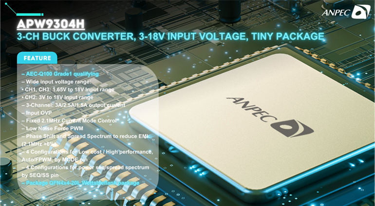
3-CH Buck Converter, 3-18V Input Voltage, Tiny Package
Features
- Channel 2 from 3V to 18V
- N-CH MOSFET (90 mΩ) for CH2/3 High Side
- N-CH MOSFET (45 mΩ) for CH1 Low Side
- N-CH MOSFET (50 mΩ) for CH2/3 Low Side
General Description
The APW9304H is a three-channel synchronous mode PWM converter with 3A continuous current capability for one channel and 2.5A continuous current capability for the other channel and 1.5A continuous current capability for the other one channel. Although the switching frequency of the APW9304H is fixed at 2.1MHz, it can also change the switching frequency via the EN/SYNC pin. The APW9304H also provides a 120-degree phase shifting technique and Spread Spectrum option to minimize the noise for reducing EMI. The output voltage of each channel can be adjusted using an external resistor divider. Other features include VIN OVP, VOUT OVP, UVP, current limit, and OTP. The internal switching frequency is set at 2.1MHz. Other features of the part include VIN OVP, OVP, UVP, Current Limit and OTP. The APW9304H is available in a TQFN 4x4-20D wettable flanks package with small size and excellent thermal capacity.
Features
- Wide input voltage range:
- Channel 2 from 3V to 18V
- 3A/2.5A/1.5A Output Current on Channel1/2/3
- Typical 0.6V ±1% Internal Reference Voltage
- Sync Pin Allows Synchronization to an External Clock from 1.8MHz to 2.4MHz
- Optimized Upper and Lower MOSFETs RDS_on for max Efficiency:
- N-CH MOSFET (90 mΩ) for CH2/3 High Side
- N-CH MOSFET (45 mΩ) for CH1 Low Side
- N-CH MOSFET (50 mΩ) for CH2/3 Low Side
- Built in OVP, UVP, Current Limit, VIN OVP and OTP
- Low Cost TQFN 4x4-20D Wettable Flanks Package
- High Performance or Low Cost Configuration, Auto Mode or FPWM can be set by MODE PIN
- Spread Spectrum Option and Power On Sequence can be configured by SEQ/SSP PIN
General Description
The APW9304H is a three-channel synchronous mode PWM converter with 3A continuous current capability for one channel and 2.5A continuous current capability for the other channel and 1.5A continuous current capability for the other one channel. Although the switching frequency of the APW9304H is fixed at 2.1MHz, it can also change the switching frequency via the EN/SYNC pin. The APW9304H also provides a 120-degree phase shifting technique and Spread Spectrum option to minimize the noise for reducing EMI. The output voltage of each channel can be adjusted using an external resistor divider. Other features include VIN OVP, VOUT OVP, UVP, current limit, and OTP. The internal switching frequency is set at 2.1MHz. Other features of the part include VIN OVP, OVP, UVP, Current Limit and OTP. The APW9304H is available in a TQFN 4x4-20D wettable flanks package with small size and excellent thermal capacity.
NEWS
Active
Ultra-Low On-Resistance, 6A Dual Load Switch With Soft Start
Features
General Description
The APL3528 is an ultra-low on-resistance, dual powerdistribution switch with external soft start control. It integrates two N-channel MOSFETs that can deliver 6A continuous load current each. The device integrates over-temperature protection. The over temperature protection function shuts down the Nchannel MOSFET power switch when the junction temperature rises beyond 160oC and will automatically turns on the power switch when the temperature drops by 40oC. The device is available in lead free TDFN2x3-14A packages.
Features
- 20mΩ (Typical) On-resistance per Channel
- 6A Continuous Current
- Soft Start Time Programmable by External Capacitor
- Wide Input Voltage Range (VIN): 0.8V to 5.5V
- Supply Voltage Range (VBIAS): 3V to 5.5V
- Output Discharge when Switch Disabled
- Reverse Current Blocking when Switch Disabled
- Over-Temperature Protection
- Enable Input
- Lead Free and Green Devices Available (RoHS Compliant)
General Description
The APL3528 is an ultra-low on-resistance, dual powerdistribution switch with external soft start control. It integrates two N-channel MOSFETs that can deliver 6A continuous load current each. The device integrates over-temperature protection. The over temperature protection function shuts down the Nchannel MOSFET power switch when the junction temperature rises beyond 160oC and will automatically turns on the power switch when the temperature drops by 40oC. The device is available in lead free TDFN2x3-14A packages.
NEWS
Active
5.5V, 7A Low RDSON Power Load Switch with Current Monitoring
Features
General Description
The APL3535 is a power-distribution switch with some protection functions that can deliver current up to 7A. The device incorporates a 12mΩ N-channel MOSFET power switch that is controlled by an enable logic pin and has a SS pin dedicated to soft start ramp-up rate control that can be used in application where the inrush current is concerned. The APL3535 integrates some protection features, including current limit protection, over temperature protection. The current limit protection can protect down-stream devices from catastrophic failure by limiting the output current at current-limit threshold during over-load or short-circuit events. The over temperature protection function shuts down the N-channel MOSFET power switch when the junction temperature rises beyond 155°C. Other features include an accurate current monitor function. The device is available in lead free QFN2x-12A package.
Features
- N-CH MOSFET RDS(ON): 12mΩ(typ.)
- Smaller than 1uA Shutdown Current
- Ultra-Low Quiescent Current: Less than 50uA
- Input Voltage Range (VIN): 0.7V ~ 5.5V
- Bias Voltage Range (VCC): 3V ~ 5.5V
- Built in Internal Charge Pump Function for Internal Gate Driver
- Built in ADJ Current Limit Function
- Built in Output Discharge Function
- Built in Adjustable Soft Start Function by SS Pin
- Built in Over-Temperature Protection
- <200ns Short-Circuitry Response Protection
- Built in Enable / Shutdown Control by EN Pin
- Built in Power Good Indication Output
- Built in IMON Function with 6% Accuracy
- Tiny Small QFN2x2-12A Package
General Description
The APL3535 is a power-distribution switch with some protection functions that can deliver current up to 7A. The device incorporates a 12mΩ N-channel MOSFET power switch that is controlled by an enable logic pin and has a SS pin dedicated to soft start ramp-up rate control that can be used in application where the inrush current is concerned. The APL3535 integrates some protection features, including current limit protection, over temperature protection. The current limit protection can protect down-stream devices from catastrophic failure by limiting the output current at current-limit threshold during over-load or short-circuit events. The over temperature protection function shuts down the N-channel MOSFET power switch when the junction temperature rises beyond 155°C. Other features include an accurate current monitor function. The device is available in lead free QFN2x-12A package.
NEWS
Active
Ultra-Low On-Resistance, Power Load Switch with Soft Start
Features
- RDS(ON)=12mΩ at VIN=3.6V
- RDS(ON)=12.3mΩ at VIN=2.5V
- RDS(ON)=12.5mΩ at VIN=1.8V
- RDS(ON)=17.5mΩ at VIN=1V
General Description
The APL3537C is an ultra-low on-resistance, power-distribution switch with internal soft start control. The device is a N-channel MOSFET which needs only one input voltage from 0.95V to 5.5V. Built in internal charge pump function biases the N-MOS switch to achieve a minimum switch on-resistance. The APL3537C can be enabled by other power system. Pulling and holding the EN pin below 0.4V shuts off the output. The device is available in lead free WLCSP 0.9x1.4-6 package.
Features
- Ultra-Low On-Resistance :
- RDS(ON)=12mΩ at VIN=3.6V
- RDS(ON)=12.3mΩ at VIN=2.5V
- RDS(ON)=12.5mΩ at VIN=1.8V
- RDS(ON)=17.5mΩ at VIN=1V
- Ultra-Low Quiescent Current: VIN=1V Condition, 10µA (Max.)
- 3A Maximum Continuous Output Current
- Supply Voltage Range from 0.95V to 5.5V
- Built in Internal Charge Pump Function for Internal Gate Driver
- Built in Internal Soft-Start Function : VIN=3.6V Condition, 800µs (Typ.)
- Built in Enable/Shutdown Control
- Built in Turn On Time : VIN=3.6V Condition, 860µs (Typ.)
- Built in Reverse Current Block Function
- Tiny small WLCSP 0.9x1.4-6 Package
- Lead Free and Green Devices Available (RoHS Compliant)
General Description
The APL3537C is an ultra-low on-resistance, power-distribution switch with internal soft start control. The device is a N-channel MOSFET which needs only one input voltage from 0.95V to 5.5V. Built in internal charge pump function biases the N-MOS switch to achieve a minimum switch on-resistance. The APL3537C can be enabled by other power system. Pulling and holding the EN pin below 0.4V shuts off the output. The device is available in lead free WLCSP 0.9x1.4-6 package.
NEWS
Active
USB Power-Distribution Switches
Features
- HBM with over 2kV
- CDM with over 500V at VIN pin
General Description
The APL3576A is designed for desktop adapter applications. The low on resistance N-channel MOSFET power switch can satisfy the voltage drop requirements of USB specification. Protection features include current-limit protection, short-circuit protection, over-temperature protection, wrong VIN input voltage protection, surge protection, and reverse current blocking. Other features include a deglitched ACOK output to indicate the fault condition and an enable input to enable or disable the device.
Features
- VIN Input Voltage Range: 4.5 to 25V
- 30V Absolute Ratings at VIN Pin
- 15A Output Current Capability
- Adjustable Soft-start Time by SS pin
- Fast Over Current Protection Response Time
- Wrong VIN Input Voltage Protection
- Fault Report on ACOK Pin
- Built-in Surge Protection when Surge Voltage over 27V
- Built-in Thermal Shutdown Protection
- Built-in Enable / Shutdown Control by DPREN Pin
- Integrated Internal Charge Pump
- Built-in Programmable Short Circuit or Over Current Protection Threshold Setting by ALSET pin
- ESD Protection:
- HBM with over 2kV
- CDM with over 500V at VIN pin
- Over-Temperature Protection
- TQFN4x4-24 Package
General Description
The APL3576A is designed for desktop adapter applications. The low on resistance N-channel MOSFET power switch can satisfy the voltage drop requirements of USB specification. Protection features include current-limit protection, short-circuit protection, over-temperature protection, wrong VIN input voltage protection, surge protection, and reverse current blocking. Other features include a deglitched ACOK output to indicate the fault condition and an enable input to enable or disable the device.
NEWS
Active
Stereo, Differential Input Cap-Free Line Driver
Features
- Save the PCB Space
- Reduce the BOM Costs
- Improve the Low Frequency Response
- Noise < 8µVrms
- THD+N < 0.02% at 20Hz~20kHz
- TSSOP-14
General Description
The APA2171 is a stereo, differential input, single supply, and cap-free line driver, which is available in SOP-14 and TSSOP-14 packages. The APA2171 is ground-reference output, and doesn’t need the output capacitors for DC blocking. The advantages of eliminating the output capacitor are saving the cost, eliminating component height, and improving the low frequency response. The external gain setting is recommended using from ±1V/ V to ±10V/V. High PSRR provides increased immunity to noise and RF rectification. APA2171 has shutdown and under-voltage detector function for Depop solution. The APA2171 is capable of driving 2.1Vrms at 3.3V into 2.5kΩ load, and provides short-circuit and thermal protection.
Features
- Operating Voltage : 3V~3.6V
- Differential Input
- Ground Reference Output
- Save the PCB Space
- Reduce the BOM Costs
- Improve the Low Frequency Response
- Low Noise and THD+N
- Noise < 8µVrms
- THD+N < 0.02% at 20Hz~20kHz
- Output Voltage Swing Can Reach 2.1Vrms/Ch into 2.5kΩ at VDD=3.3V
- High PSRR : 80dB at 217Hz
- Fast Start-up Time : 500µs
- Integrate the De-Pop Circuitry
- Thermal and Short-Circuit Protection
- Surface-Mount Packaging
- TSSOP-14
- Lead Free and Green Devices Available (RoHS Compliant)
General Description
The APA2171 is a stereo, differential input, single supply, and cap-free line driver, which is available in SOP-14 and TSSOP-14 packages. The APA2171 is ground-reference output, and doesn’t need the output capacitors for DC blocking. The advantages of eliminating the output capacitor are saving the cost, eliminating component height, and improving the low frequency response. The external gain setting is recommended using from ±1V/ V to ±10V/V. High PSRR provides increased immunity to noise and RF rectification. APA2171 has shutdown and under-voltage detector function for Depop solution. The APA2171 is capable of driving 2.1Vrms at 3.3V into 2.5kΩ load, and provides short-circuit and thermal protection.
NEWS
Active
5 Buck Converters and 1 Termination LDO PMIC with I2C Interface
Features
- 1.5A output current capability
- 750KHz / 1.5MHz switching frequency
- 1.5A output current capability
- 750KHz / 1.5MHz switching frequency
- 1.0A output current capability
- 750KHz / 1.5MHz switching frequency
- 1.0A output current capability
- 750KHz / 1.5MHz switching frequency
- 1.0A output current capability
- 750KHz / 1.5MHz switching frequency
General Description
The APW6016E is designed for server management processor power system, which integrates 5 buck converters and one 0.5A sink/source VTT LDO into one single package. The PWM converters and VTT LDO output voltage can support VCORE, memory, memory bus termination and 1.8V/2.5V/3.3V I/O. Each VR voltage are programmable with high resolution via I2C interface. Moreover, the power-on and power-off sequences as well as soft-start time of these VR are controlled and programmable via I2C interface, providing versatility for system designers. The APW6016E provides excellent transient response and accurate DC voltage output in either PFM or PWM Mode. In Pulse Frequency Modulation mode (PFM), the APW6016E provides very high efficiency over light to heavy loads with loading-modulated switching frequencies. On VTQFN-32 Package, the Forced PWM Mode works nearly at constant frequency for low-noise requirements. The APW6016E features sufficient protections against over-current, over-voltage, short circuit and over temperature to prevent catastrophic failure. A Power-On- Reset function monitors the voltage on SVIN prevents wrong operation during power on. The output voltage of VTT automatically tracks the voltage of half VOUT2. The VTT output voltage is only requiring 10µF of ceramic output capacitance for stability and fast transient response.
Features
- High Input Voltages Range from 4.5V to 16V
- Built in Input Voltage UVLO threshold
- Built in VIN OVP
- Programmable power sequence control by I2C for all channel
- Provide 5 Single-Buck PWM Converter and 1 Termination LDO Regulator
- Channel 1 Synchronous Buck for VCORE
- (Default 1V)
- 1.5A output current capability
- 750KHz / 1.5MHz switching frequency
- Channel 2 Synchronous Buck for Memory (Default 1.2V)
- 1.5A output current capability
- 750KHz / 1.5MHz switching frequency
- Channel 3 Synchronous Buck for I/O (Default 1.8V)
- 1.0A output current capability
- 750KHz / 1.5MHz switching frequency
- Channel 4 Synchronous Buck for I/O (Default 2.5V)
- 1.0A output current capability
- 750KHz / 1.5MHz switching frequency
- Channel 5 Synchronous Buck for I/O (Default 3.3V)
- 1.0A output current capability
- 750KHz / 1.5MHz switching frequency
- Channel 6 VTT Termination LDO Regulator
- Built-in EN function
- Built-in RST to monitor output voltage status
- Built-in Current Limit/SCP/OVP/OTP
- VTQFN-32 4mmx4mm Thin package
- Lead Free Available (RoHS Compliant)
General Description
The APW6016E is designed for server management processor power system, which integrates 5 buck converters and one 0.5A sink/source VTT LDO into one single package. The PWM converters and VTT LDO output voltage can support VCORE, memory, memory bus termination and 1.8V/2.5V/3.3V I/O. Each VR voltage are programmable with high resolution via I2C interface. Moreover, the power-on and power-off sequences as well as soft-start time of these VR are controlled and programmable via I2C interface, providing versatility for system designers. The APW6016E provides excellent transient response and accurate DC voltage output in either PFM or PWM Mode. In Pulse Frequency Modulation mode (PFM), the APW6016E provides very high efficiency over light to heavy loads with loading-modulated switching frequencies. On VTQFN-32 Package, the Forced PWM Mode works nearly at constant frequency for low-noise requirements. The APW6016E features sufficient protections against over-current, over-voltage, short circuit and over temperature to prevent catastrophic failure. A Power-On- Reset function monitors the voltage on SVIN prevents wrong operation during power on. The output voltage of VTT automatically tracks the voltage of half VOUT2. The VTT output voltage is only requiring 10µF of ceramic output capacitance for stability and fast transient response.
NEWS
Active
Three-Phase Full-wave Sine-wave Brushless Motor Driver
Features
General Description
The APX9323B is a three-phase full-wave sine-wave brushless motor drive by sensor-less. This IC built-in direct PWM input speed control, current limit and soft start features suitable for the three-phase brushless DC motors. The APX9323B is available in VTDFN3x3-10 package (see Pin Configuration).
Features
- Three-Phase Full-Wave Sine-Wave Driver
- Sensor-Less Driver Control
- PWM Speed Control
- Minimum Speed Setting
- Power Saving Function
- Built-in 5V LDO Regulator
- Built-in Current Limit Circuit
- Built-in Over Current Protection
- Built-in Lock Protection and Auto Restart Function
- Soft Start Function
- FG, 1/2FG, RD or 1/3FG Output
- Built-in Thermal Shutdown Protection
General Description
The APX9323B is a three-phase full-wave sine-wave brushless motor drive by sensor-less. This IC built-in direct PWM input speed control, current limit and soft start features suitable for the three-phase brushless DC motors. The APX9323B is available in VTDFN3x3-10 package (see Pin Configuration).
Application

為消費性、可攜式/IOT和車用電子產品,提供單獨高壓DC/DC電源解決方案和高整合/客製化 PMICs
提供低元件數量設計和低靜態電流的特性,是空間受限的 PCBs 和電池供電應用的理想選擇

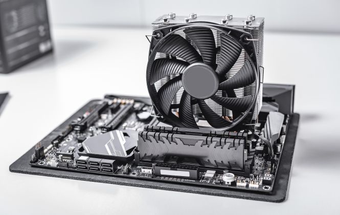
茂達電子為汽車電子提供了完整的電源解決方案,規劃支援輸入電壓範圍從 3V 到 42V,並提供輸出電流範圍從 1A 到 6A。
此外,茂達電子致力於降低 EMI (Out-of-Phase operation & Spread spectrum),並提供...
About Us
品質保證 是茂達對社會的承諾
茂達電子成立於1997年10月,為台灣第一家掛牌之Power IC (功率積體電路) 設計公司。為滿足高端市場需求,茂達電子於2000年啟動轉型,大幅建置數位/混合 IC 設計能量與相關產品線,成為Power-based mix-signal IC 供應商,提供客戶完整的Mix-signal IC 解決方案。

持續改善

客戶滿意

品質承諾

全員參與

精準到位

DATE
2024/04/24
產品訊息
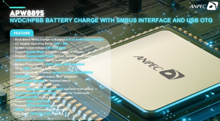
Discover the APW8895: a Synchronous NVDC Buck-Boost Switching Charger Controller
Discover the APW8895: a Synchronous NVDC Buck-Boost Switching Charger Controller.

DATE
2024/04/08
產品訊息
ANPEC Collaborates with Valens Semiconductor to Deliver Optimized Automotive Power Solutions
We are thrilled to announce a collaboration between ANPEC and Valens to develop cutting-edge solutions for the automotive industry. The companies collaborated on integrating ANPEC's APW9304H, an AEC-Q100 qualified Power Management IC, known for its ultra-low EMI feature and flexible power sequencing, to Valens' VA7000 and VA6000 series product reference designs for ADAS, autonomous driving and in-car entertainment systems.

DATE
2024/01/12
產品訊息
APW9304H is an ultra-low EMI triple buck converter and designed for automotive applications (AEC-Q100)
Meet the APW9304H, an advanced triple buck converter designed for automotive excellence (AEC-Q100).


DATE
2023/03/26
社會參與
【環境保護】竹北水月公園淨灘
茂達電子的同仁其中有部分成員攜帶家中小朋友一同共襄盛舉,淨灘時面對需要攀爬堤防的地形毫無懼色,更是爭先恐後地往遠處及靠近河口的泥濘處移動,只為了撿取更多垃圾!垃圾主要分布為寶特瓶、玻璃瓶、鐵鋁罐及塑膠袋等各種民生用品及保麗龍漁具、漁業用浮球等。大人及小孩合計46人參與本次活動,共清除283公斤海洋廢棄物。